This too had signs that it had been someones repair project in the past. The CPU had been removed and replaced by a tatty looking, badly fitted CPU socket.
The soldering on the reverse was a mess, gloopy soldering, smears of solder splashes everywhere...
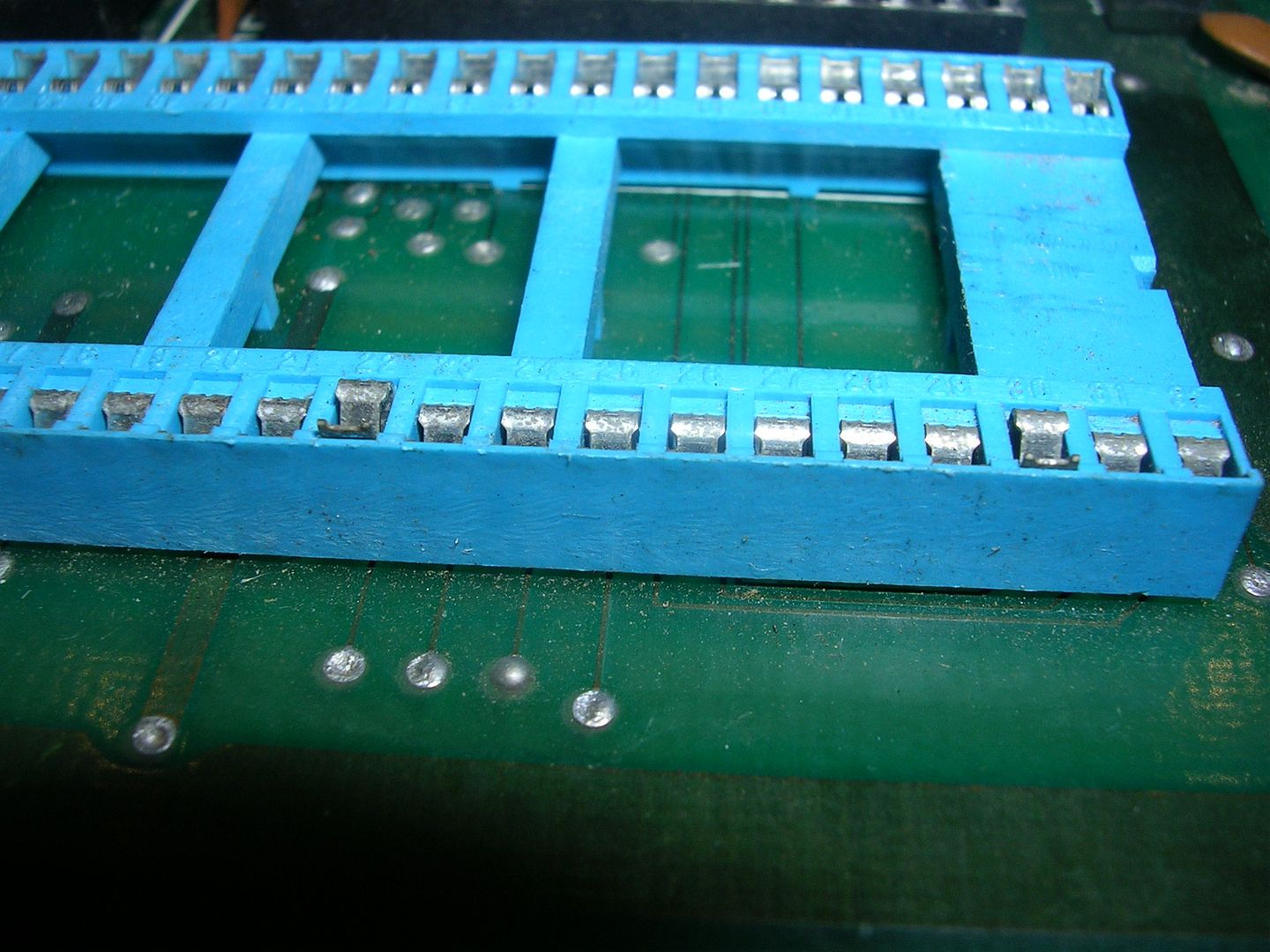
... and some of the socket pins were not visible through the board They had been pushed out of the plastic housing when the socket was forced down onto the board with only partially cleared plate through holes.
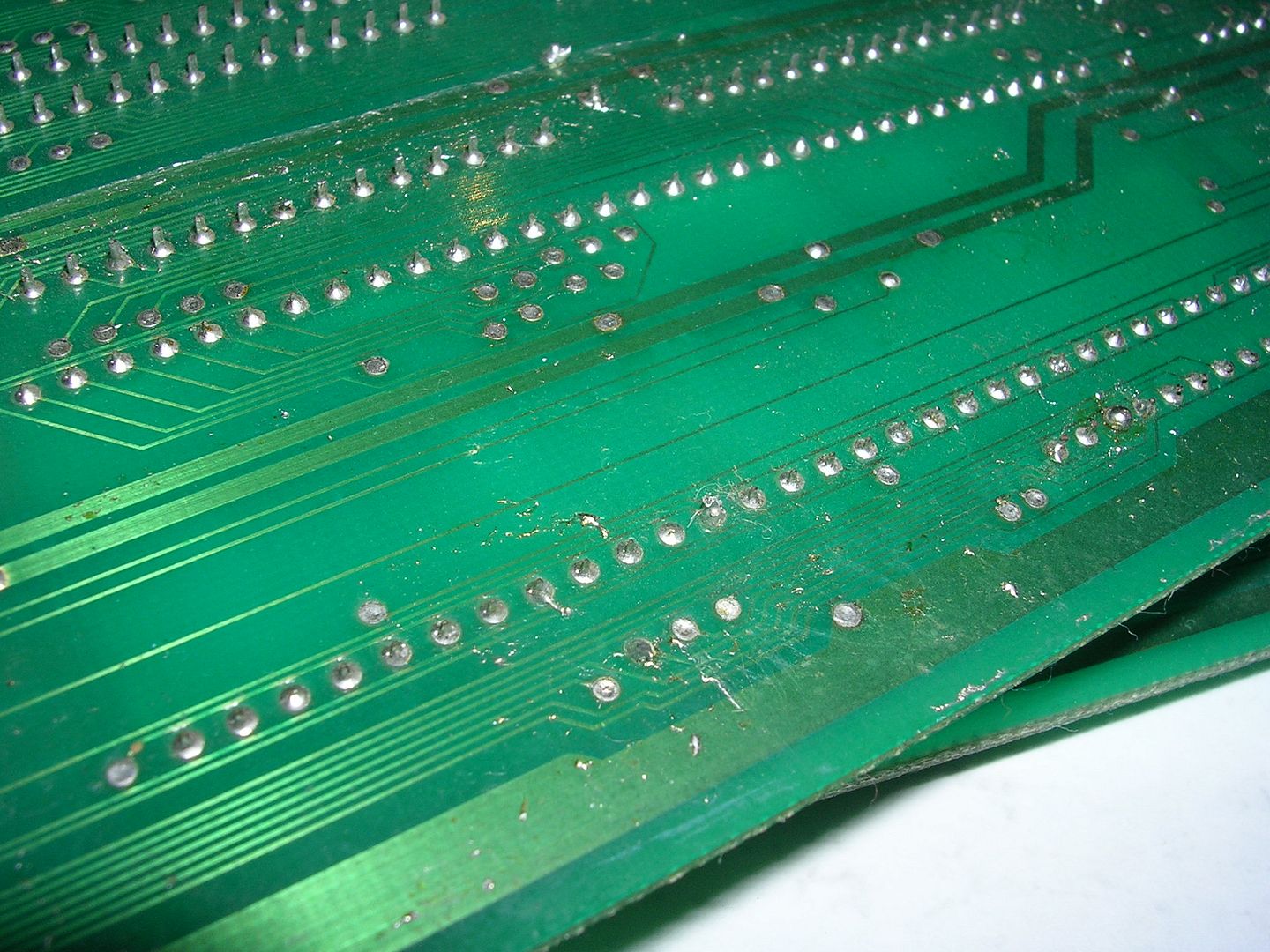
The PCB interconnects had their soldering touched up with is a tell tale sign that the previous repairer had absolutely no idea what they were doing.
This makes it hard to tell what's a good joint and what isn't, in reality you are more likely to make a good joint bad, than to somehow find an invisible bad joint and score a win.
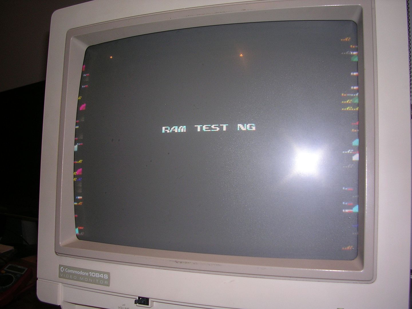
Just to see what it would do in its original state I fitted a salvaged 16Mhz crystal, swapped in the known good ROM set, dropped in the sprite PAL and powered it up. All I got was black screen and no sound beyond the amplifier hum. While poking the various CPU bus lines I did get a few coloured lines on the screen for a fraction of a second, and some random bang and ping sound effects through the speaker.
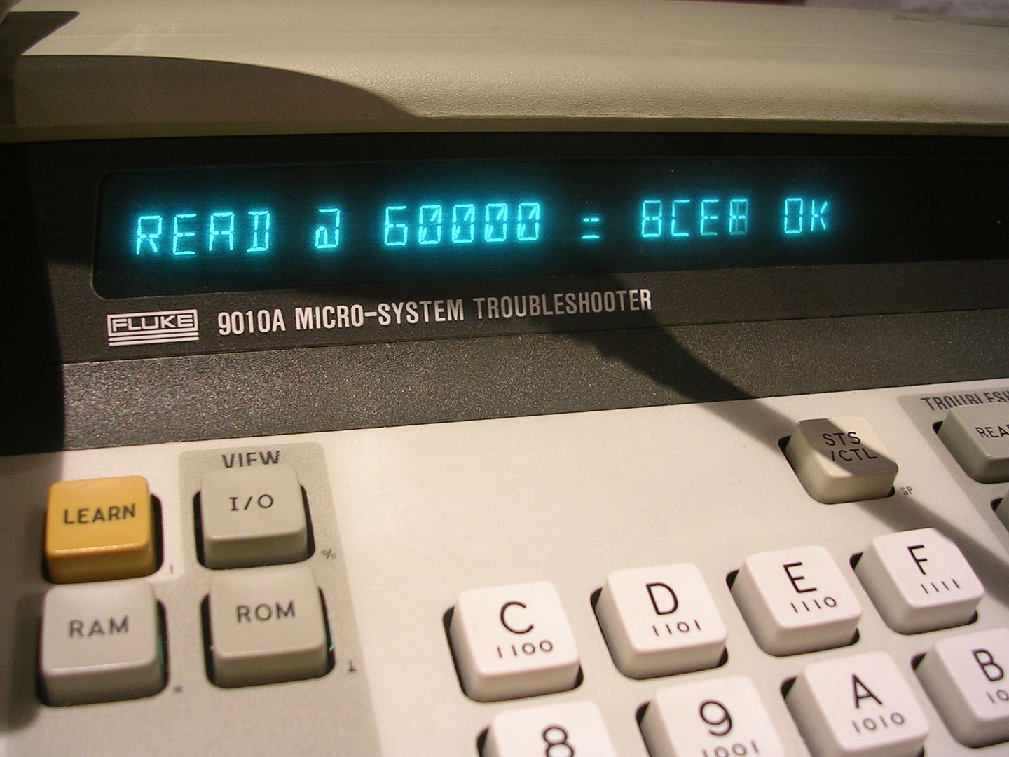
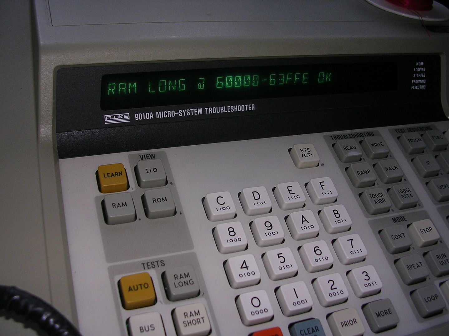
As the fluke was set up already and I now knew the ROM checksums from the other board I hooked it up and went straight to sniff the RAM. This gave and instant Read/Write fail at 0x60000 the first location in the RAM space. Setting the test to loop constantly gave a blur of changing read back results.
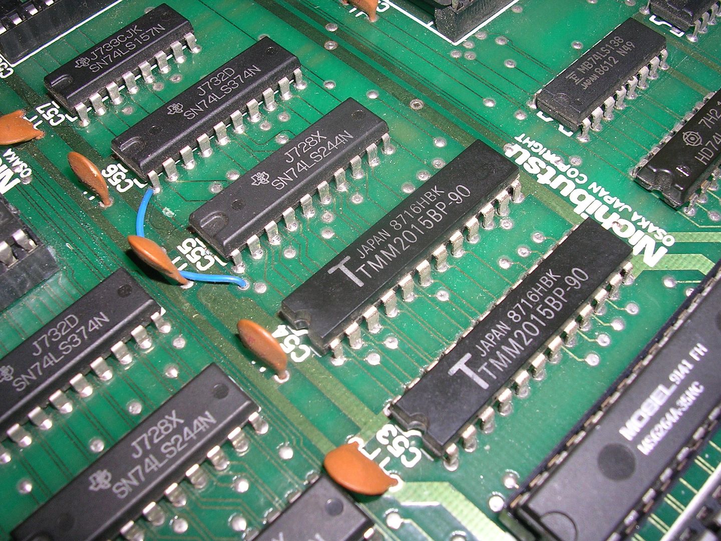
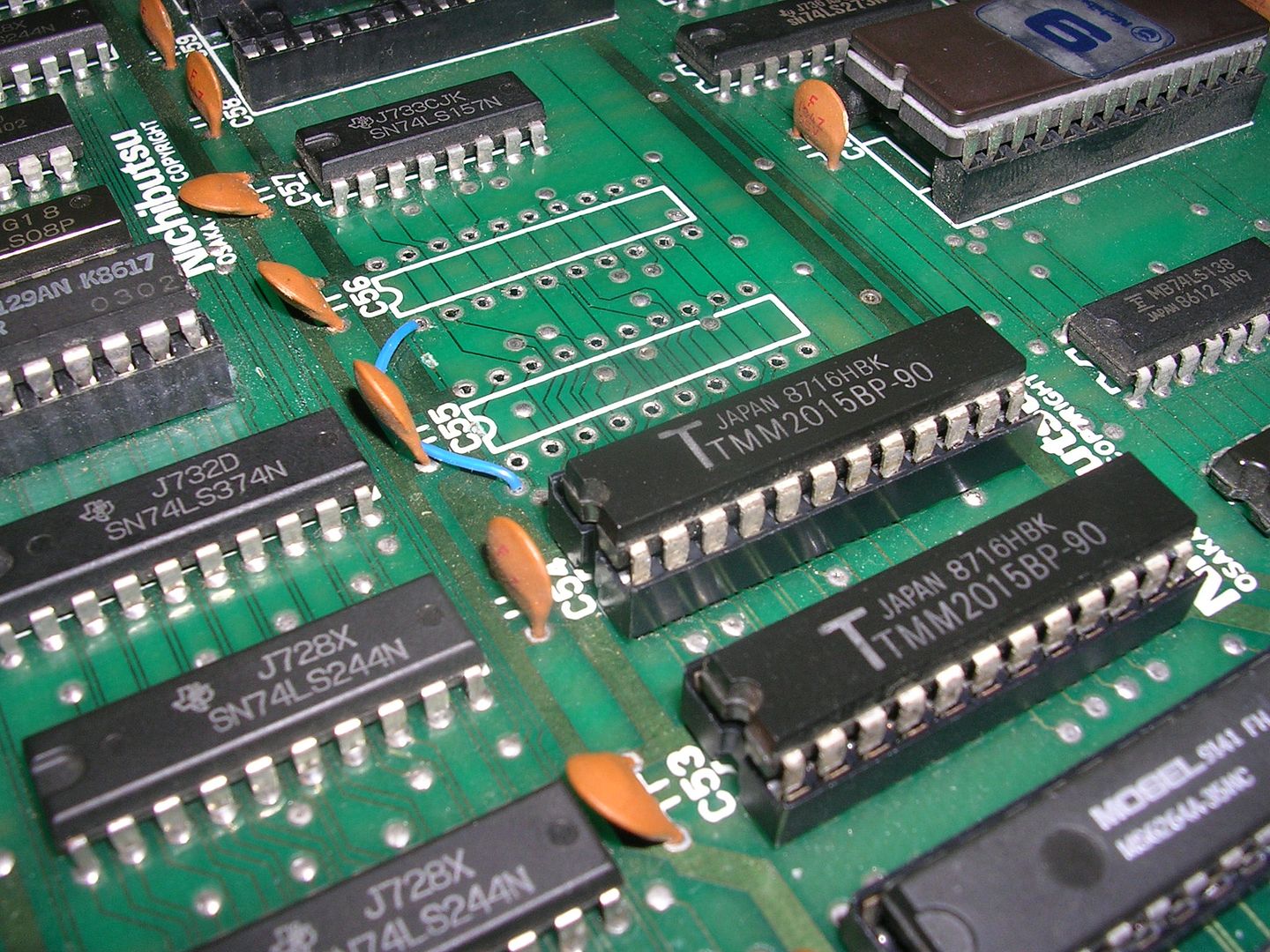
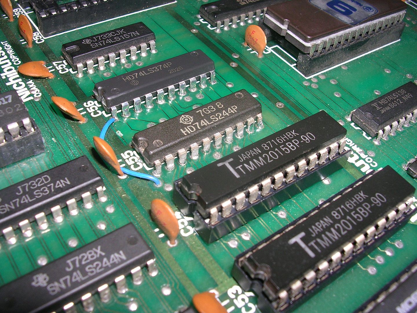
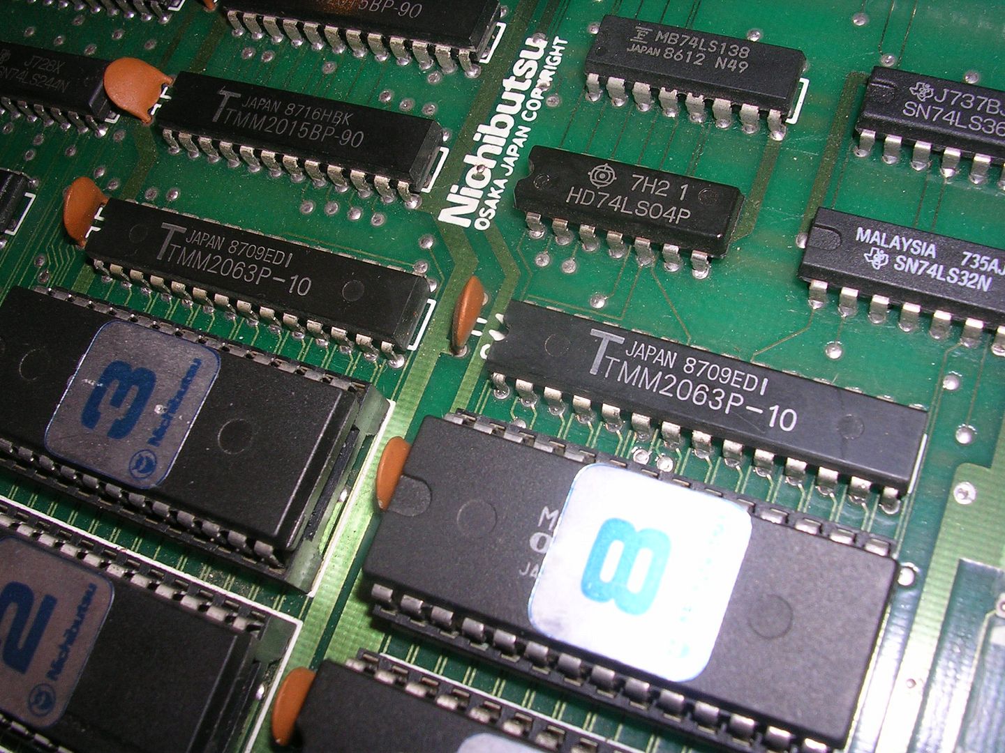
The RAM was another pair of TMM2063 ICs which if not dead are likely to be flaky, so I removed them.
This board clearly wanted to be repaired as the desoldering was so easy that with a single pass the chips would literally fall out of the board.
The TMM2063s passed their off board tests, and I have no problem putting them back on the board in sockets when the repair is complete, but when troubleshooting they bring too much risk off adding craziness if they decide to play up or fail mid way through.
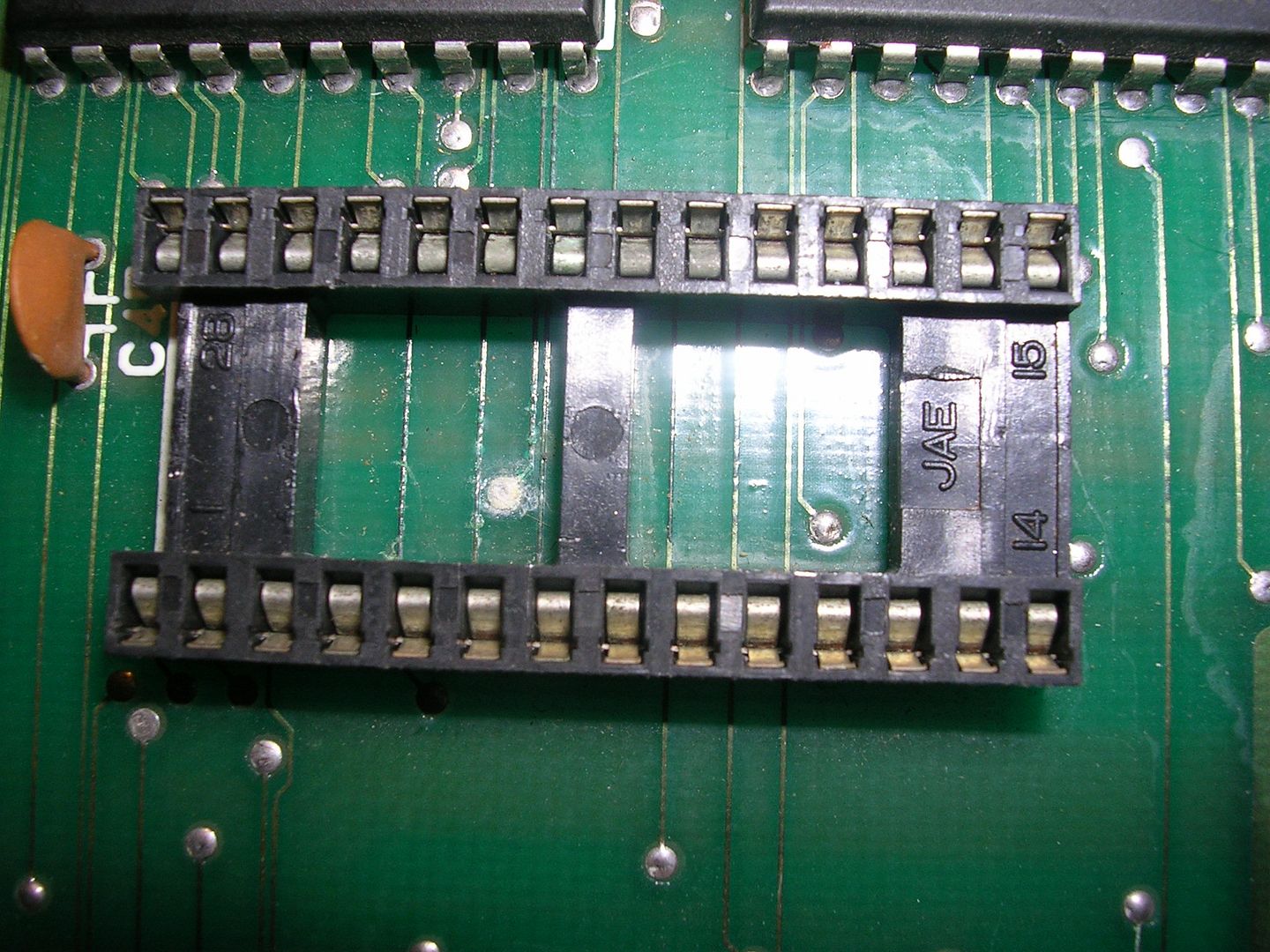
As desoldering was so easy going I took the CPU socket off to see what horrors lay beneath.
Turns out not much...
...especially after a good clean up.
Whoever desoldered the original CPU did a very good job but whoever soldered in the 64 pin socket did a horrible job, so I guess that someone guessed the fault must be a dead CPU, and took it off the board only to find it worked elsewhere and then gave up. So it ended up in someones scrap bin until someone else tried to fix it at a later date.
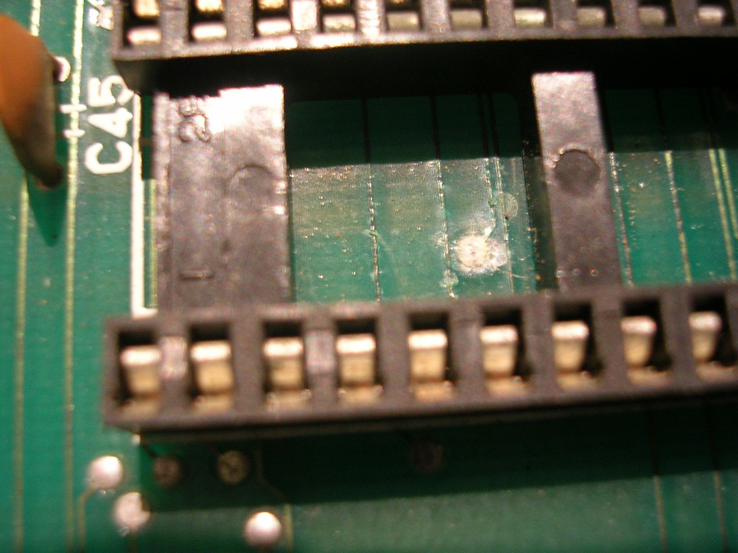
With no signs of track damage and the socket off the board I could straighten all the socket pins, realign the two pins that had been pushed out of the socket housing, give it a good clean up...
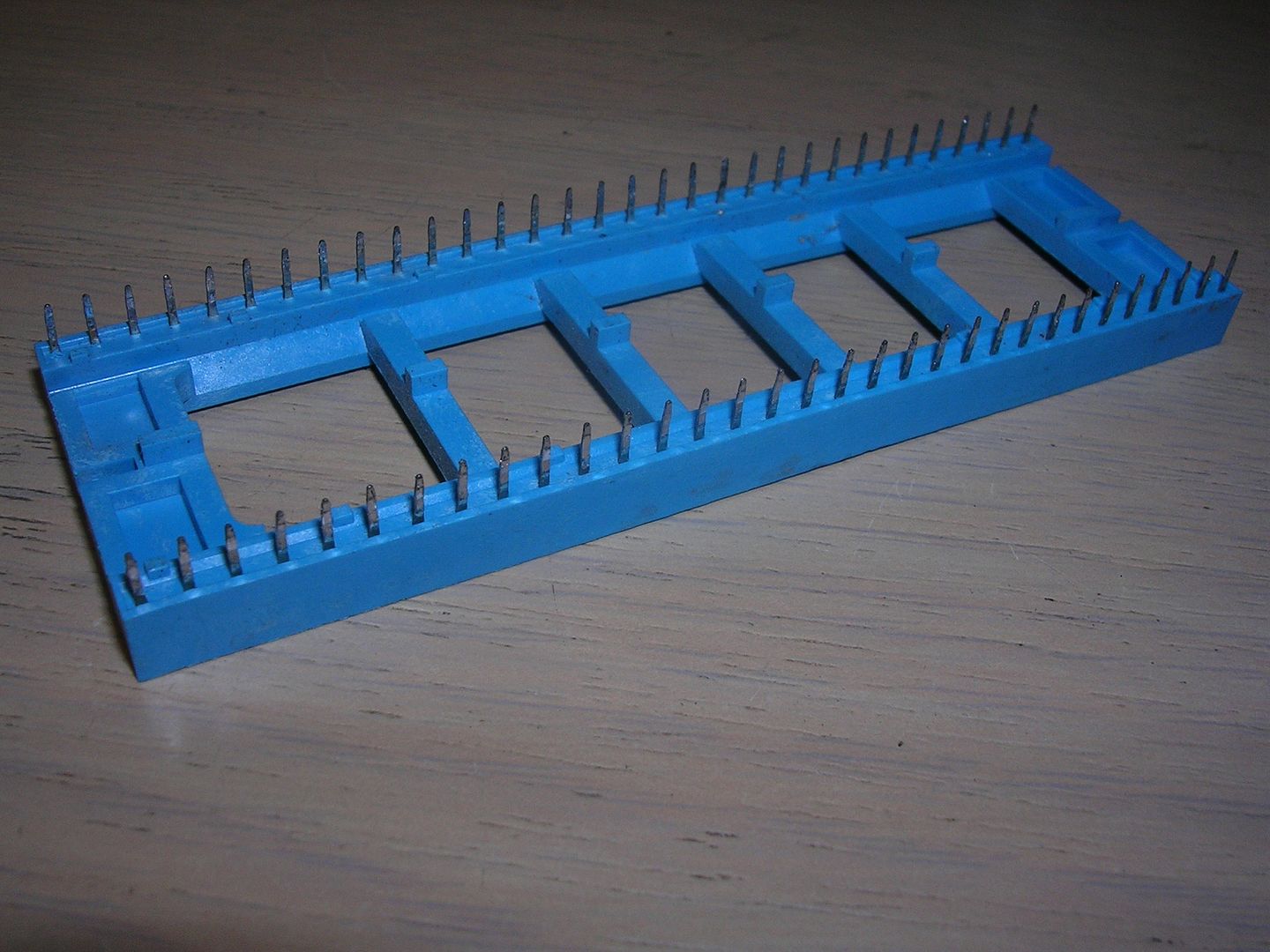
...and reinstall it, I am totally out of 64 pin IC sockets and they are hard to find these days in anything other than SDIP format. I also removed and tidied up the resistor network nearby as this was fitted at a strange angle and badly soldered.
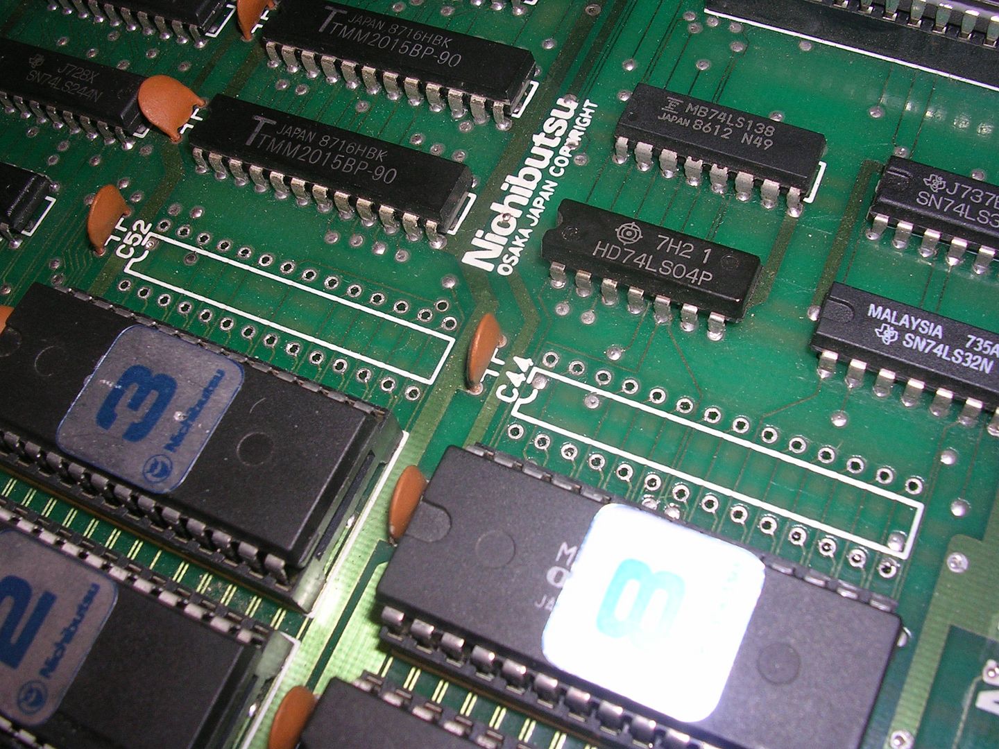
With a pair of 28 pin sockets for the RAM and the known good 6264 RAMs from PCB #1 on board I put the fluke back on, and got the same result - constant read/write errors and a blur of changing readback results.
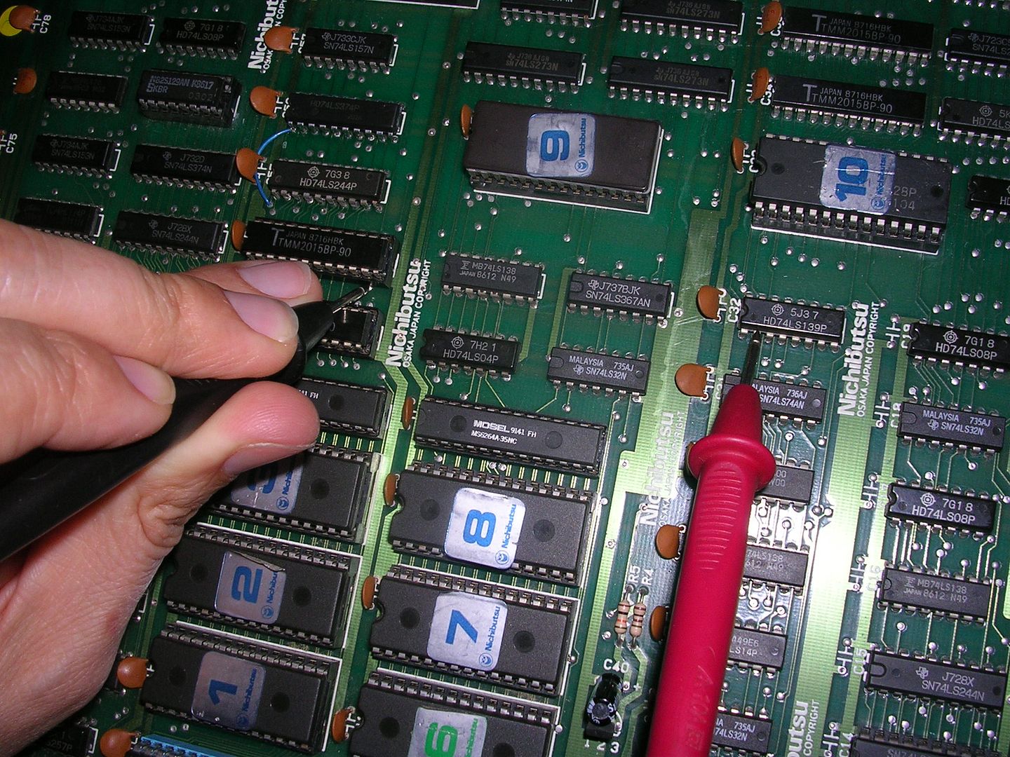
The issues clearly weren't related to the TMM2063s. If I wrote FFFF to 0x60000 and tried to read it back, I did get FFFF back, same with 0x5555, but With the test on continuous read loop it was a blur of random results. When I stopped the loop I did get FFFF back most of the time when doing it manually (ie much slower than the Fluke). I moved onto the chip select system with the scope, which is controlled by a nearby 74LS138. With the HP logic comparator connected to that IC as well as the fluke running its loop test I could look for any misbehaving address decoding that would have the effect of sending reads to the wrong block of address space giving read backs from ROM rather than RAM. It reported no weird behaviour compared to a known good 74LS138 it had on board.
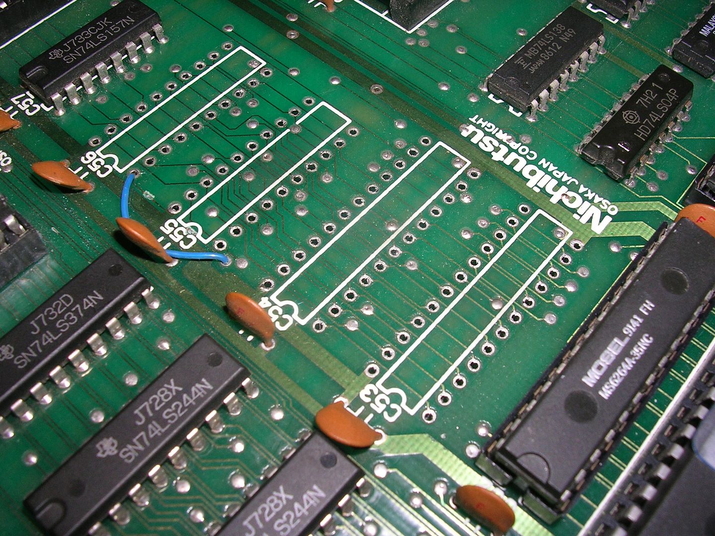
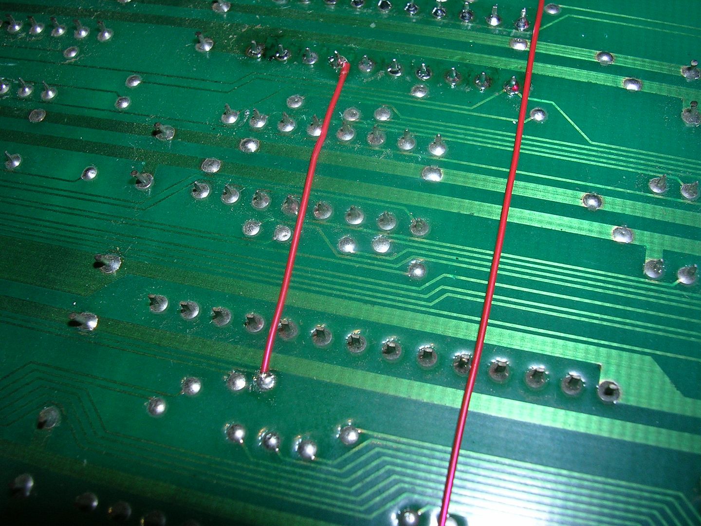
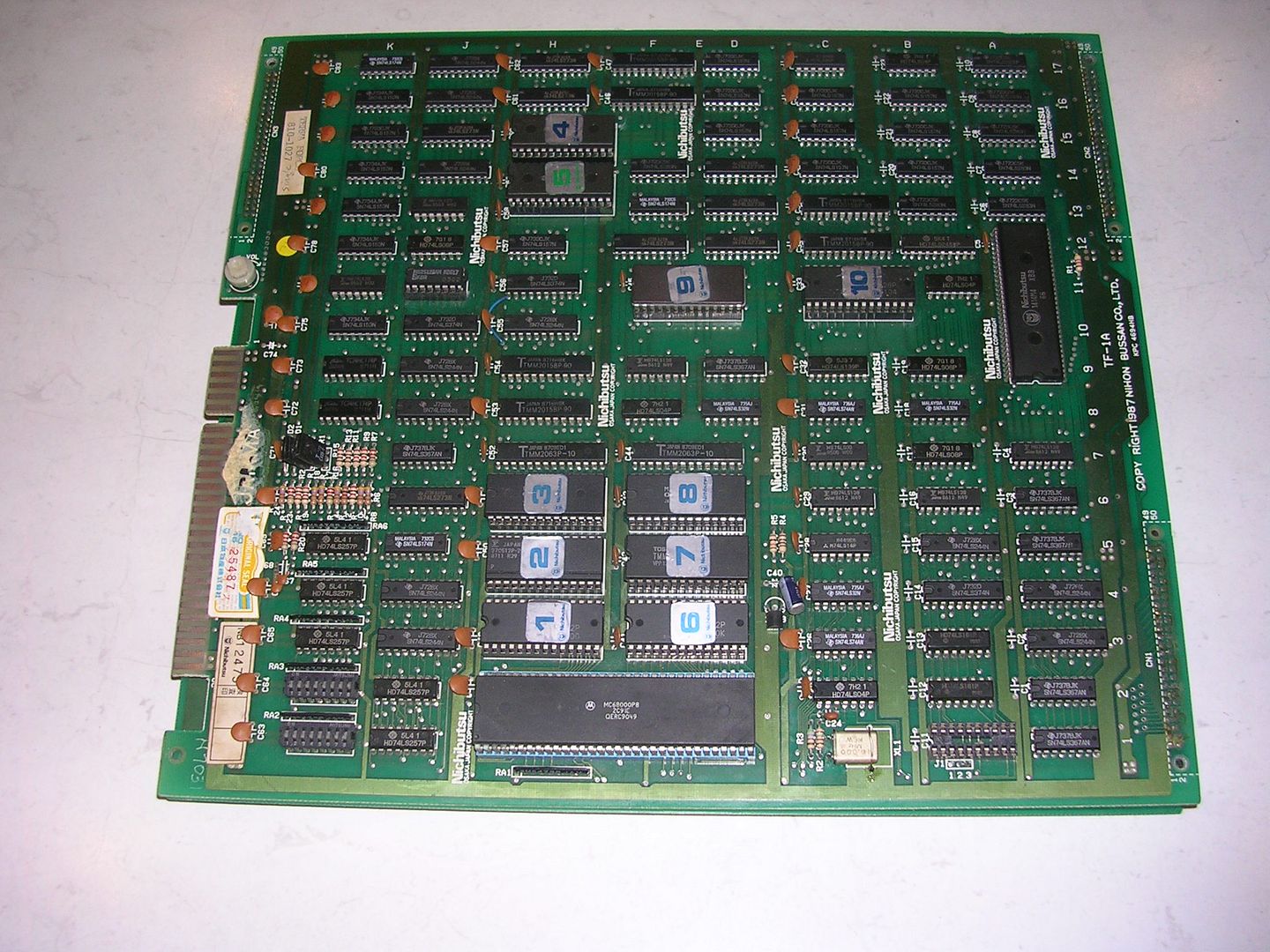
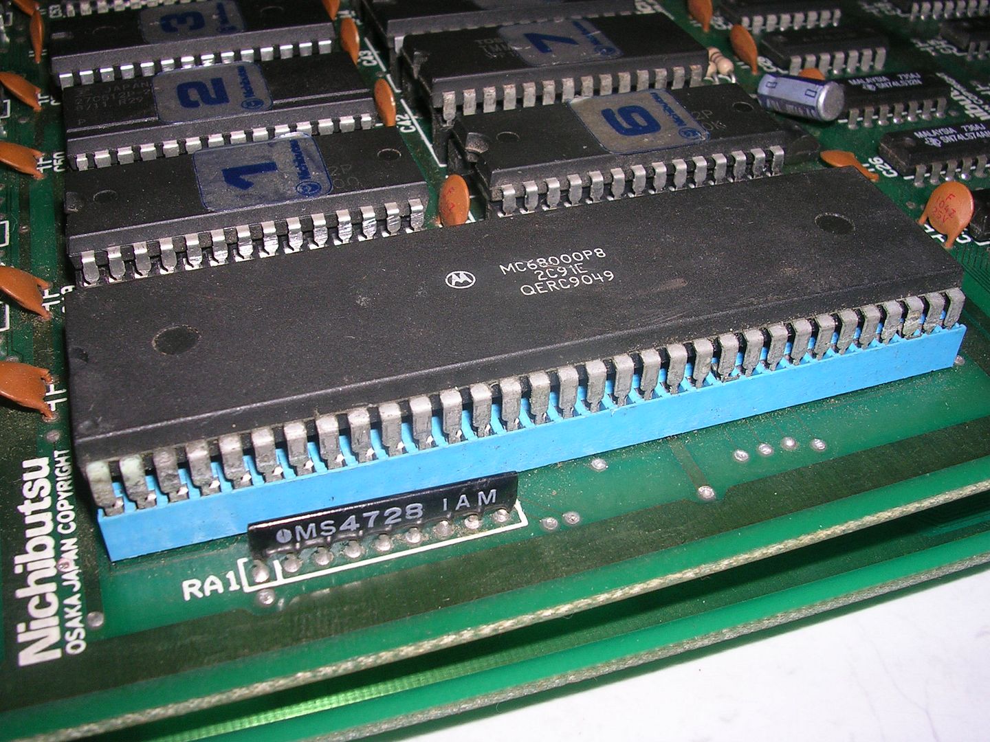
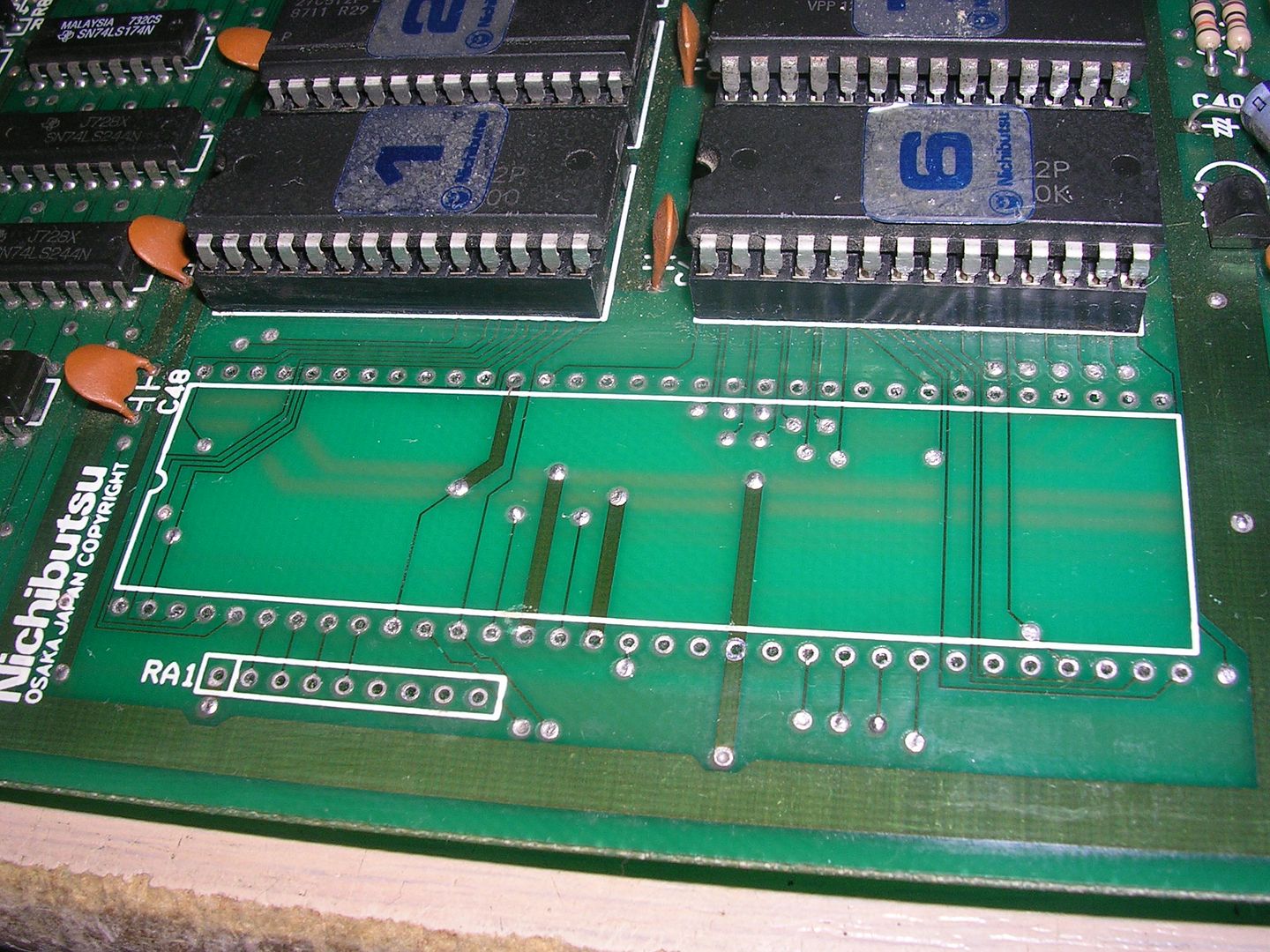
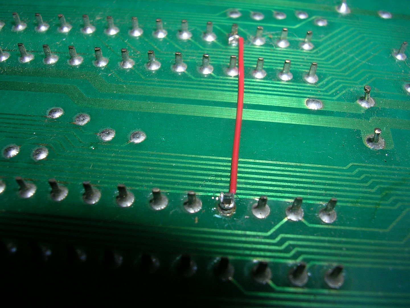
Time to buzz out the buses, and it didn't take long to find a fault, the A3 line only connected ROMs 6 and 7 to the CPU, but not the RAM or ROMS 1,2,3 or 8. As I had photos of what was under the RAM and the CPU socket I could recheck that I hadn't missed any damage. As the bus lines seem to take a U shaped path from the CPU, up the right-hand 3 ROMs, across the two RAMs and back down through the right hand ROMs I had to have an open track between the 7 and 8 ROM sockets. I think at the right angle you can just see a dark dot on the trace as it goes under the silk screening which is probably the rot spot. Am fairly sure this board got wet and water stayed under a number of IC sockets longer than elsewhere causing corrosion.

With nothing driving the A3 input across a number of ICs it was left floating and can wander about voltage wise depending on what the rest of the IC is doing. So sometimes it was a valid logic status and other times not, so the actual address being written to in the RAM would change over time, giving the random read-back failures, but ones that were hard to catch doing manual read/writes.
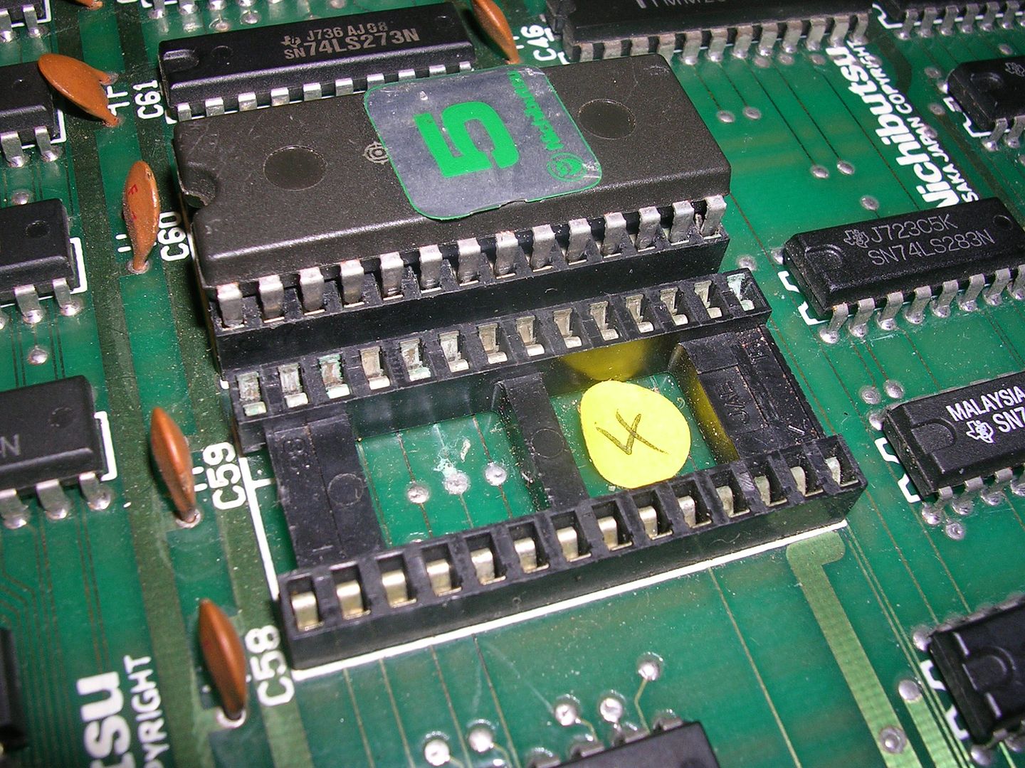
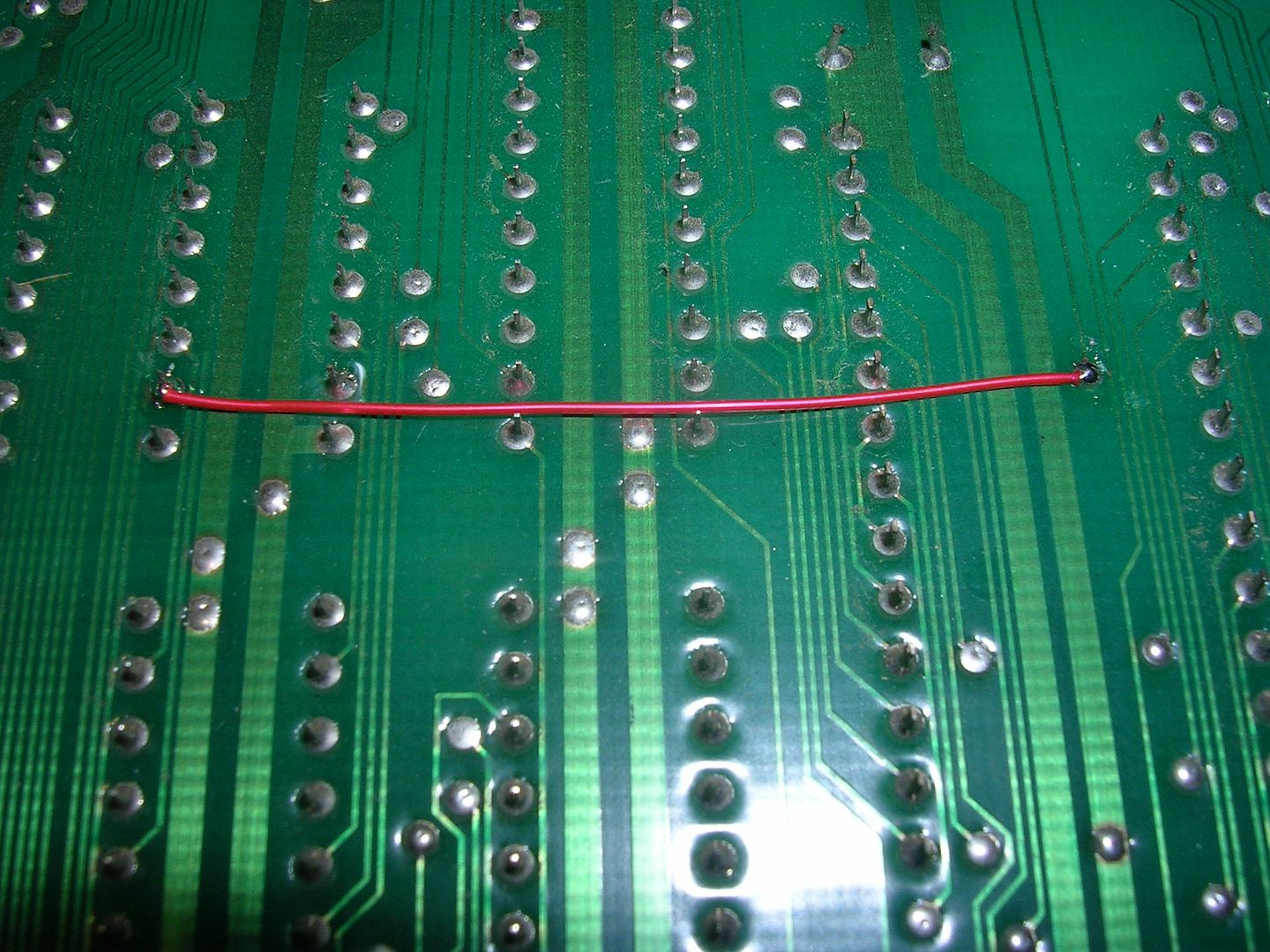
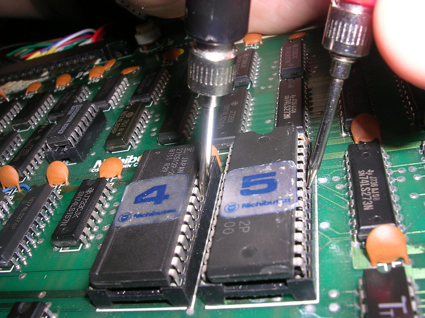
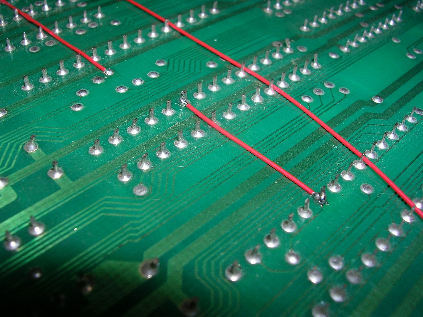
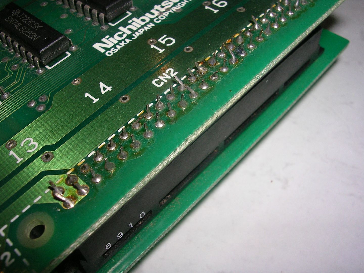
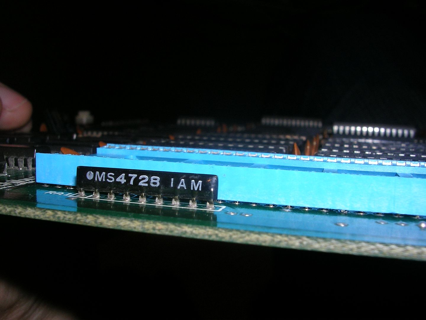
After fitting some hookup wire between these ROM sockets ...
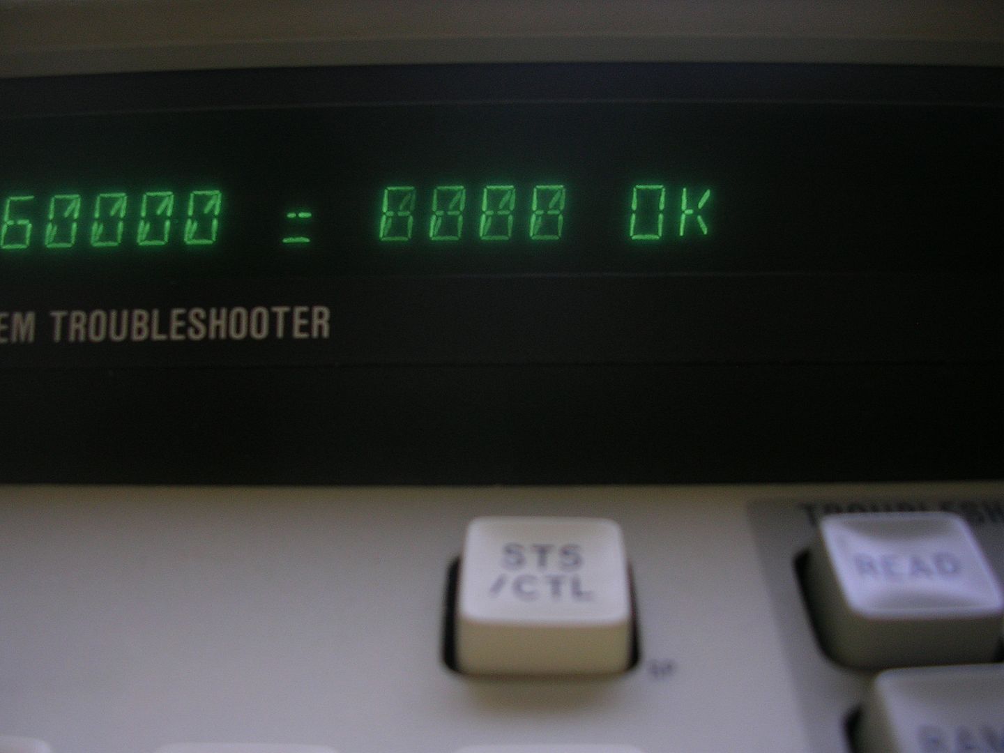
...I hooked the fluke up and re-ran the tests. All read/writes to RAM were now stable, the board even passed the "Long RAM Test" which is designed to flush out even the weirdest decoding issues.
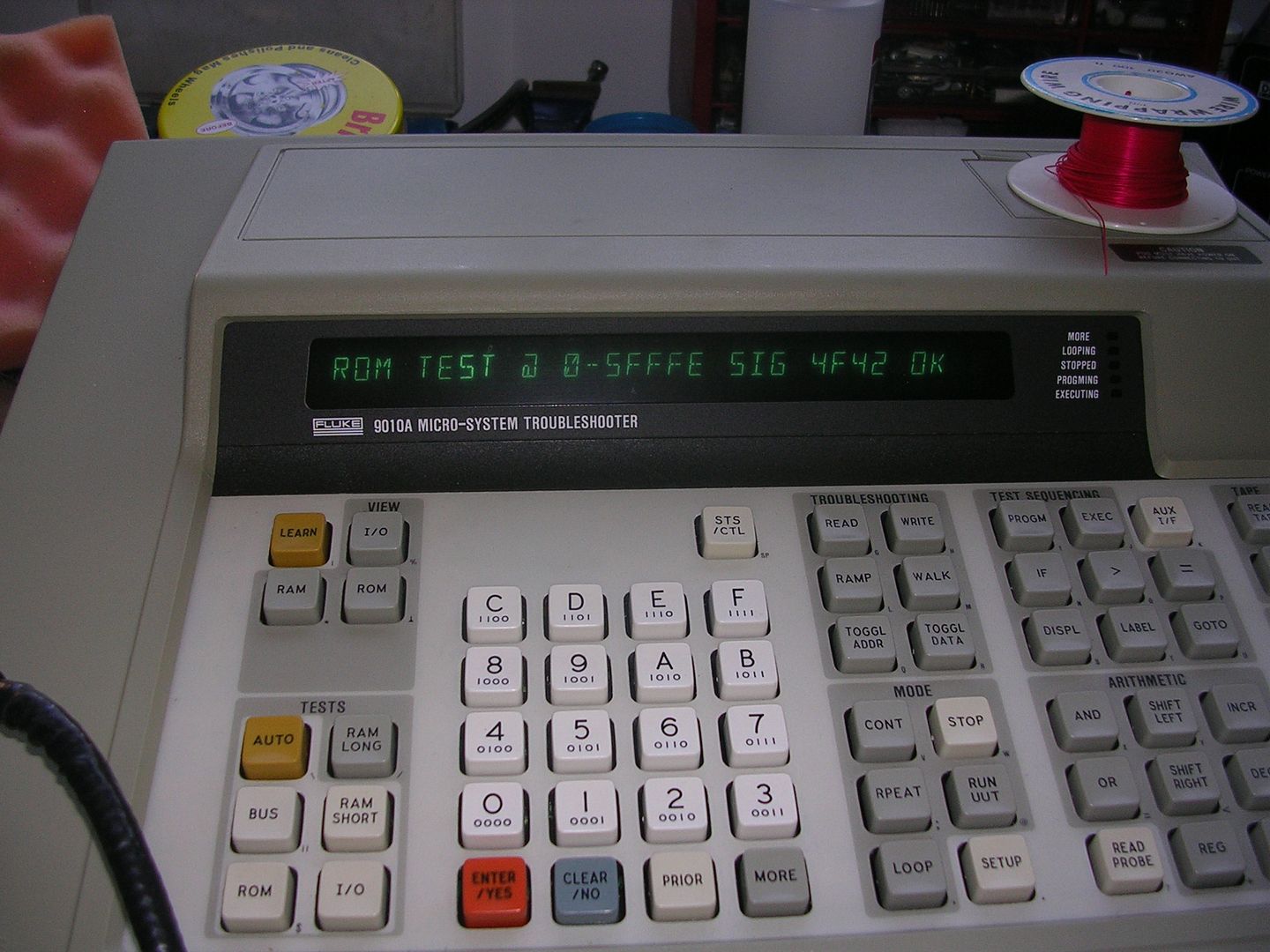
It could also calculate the correct signature from the entire set 6 CPU ROMs, proving the CPU buses were all working fine.
This should mean the board would at least boot and do something, except it didn't, it was still stone dead.
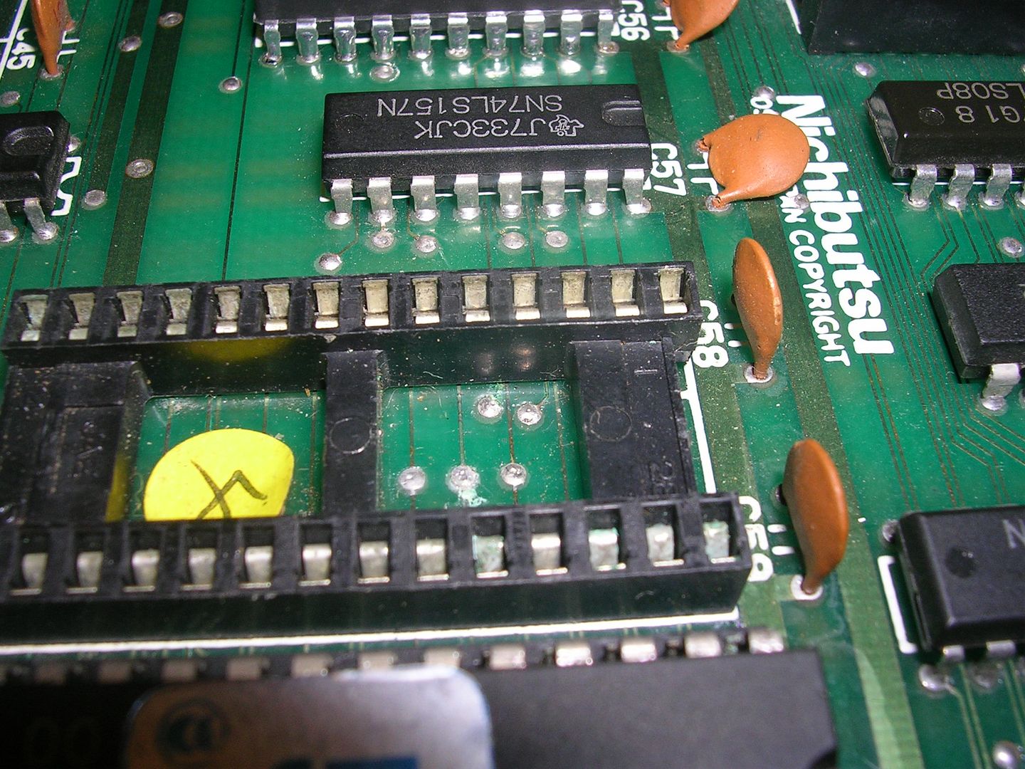
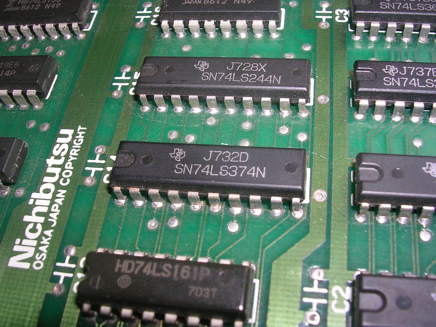
With scope data lines on ROMs were still mashed, the most likely cause for the widespread nasty signals was that the CPU had simply crashed, this can leave the bus pins in weird states that look like something horrible has happened external to the CPU. There isn't much directly on the buses outside the RAM, ROMs, CPU some LS244s and the LS347 at B4 that caused problems on the other board.
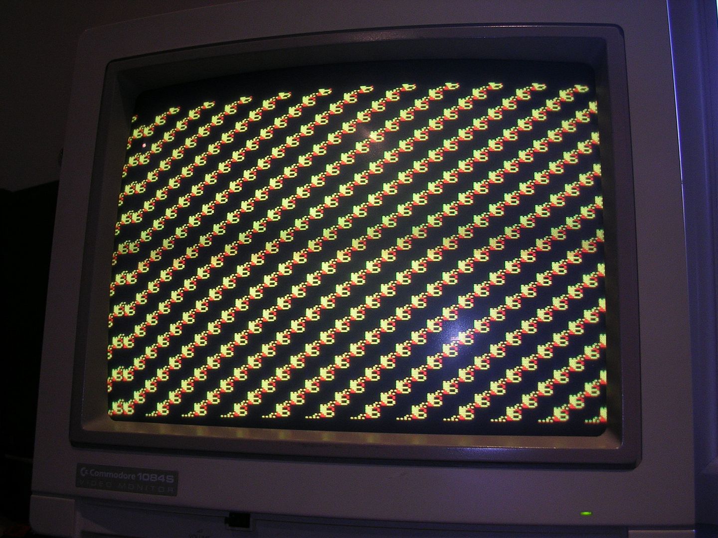
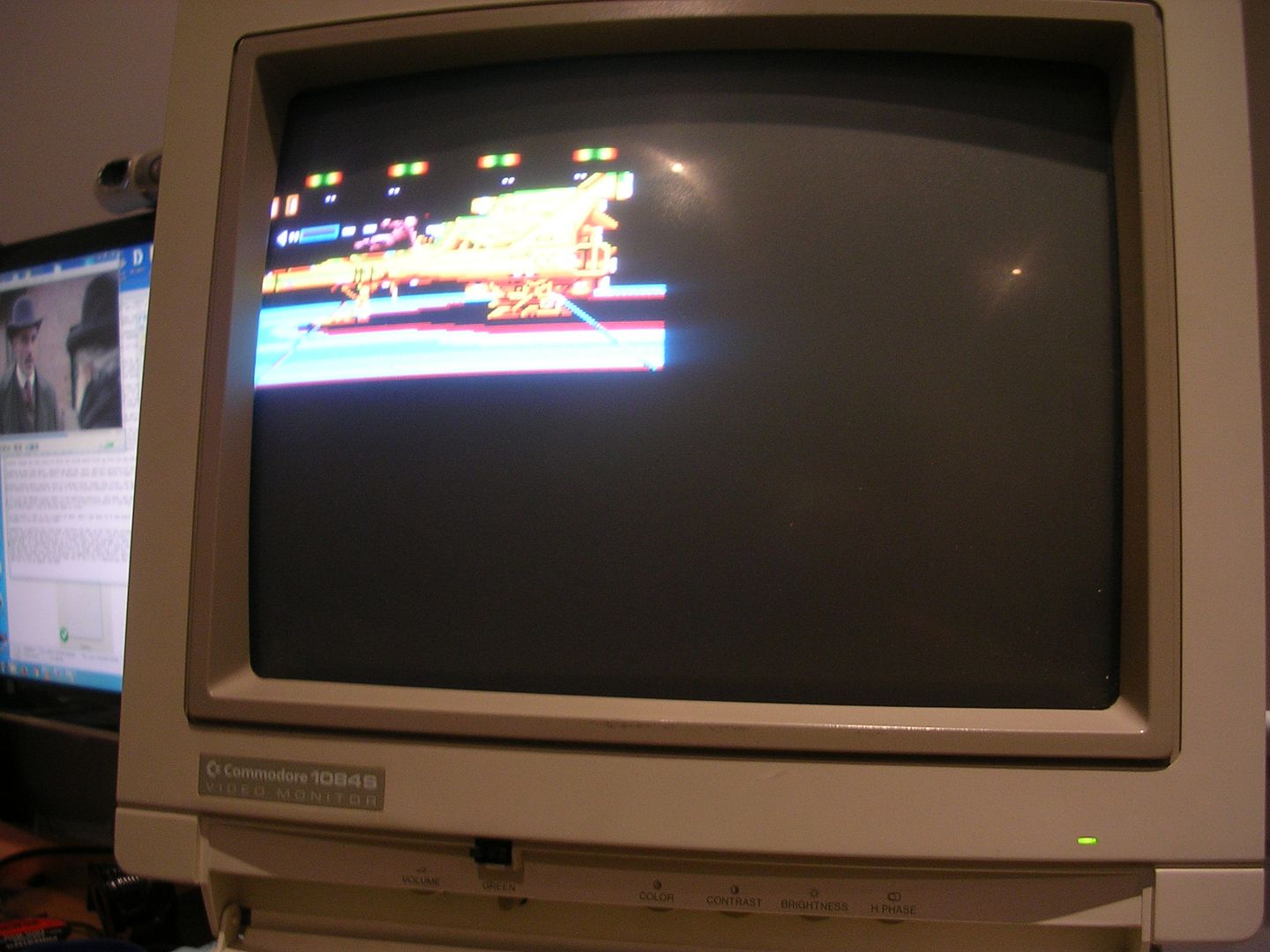
It had active inputs but vague outputs on a number of gates, so I took it off the board. The PCB can run without this as it just disconnects a large lump of the spite graphics system. With the IC removed the board still gave a black screen but started to produce a cacophony of sound effects and long sections of background music. It started playing the theme tune early on and it sounded like it was playing blind, but the effects and music were just random, its junk data going to the sound CPU that it is interpreting as instructions to play music track X or sound effect Y, at least the sound system seems to be working. The 74LS374 tested OK on my EPROM reader by I am not over confident in it, it is possibly a coincidence that a degree of life returned when it was removed but possibly not.
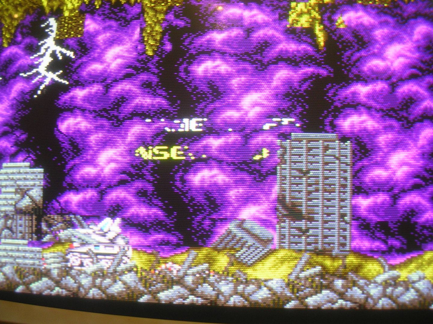
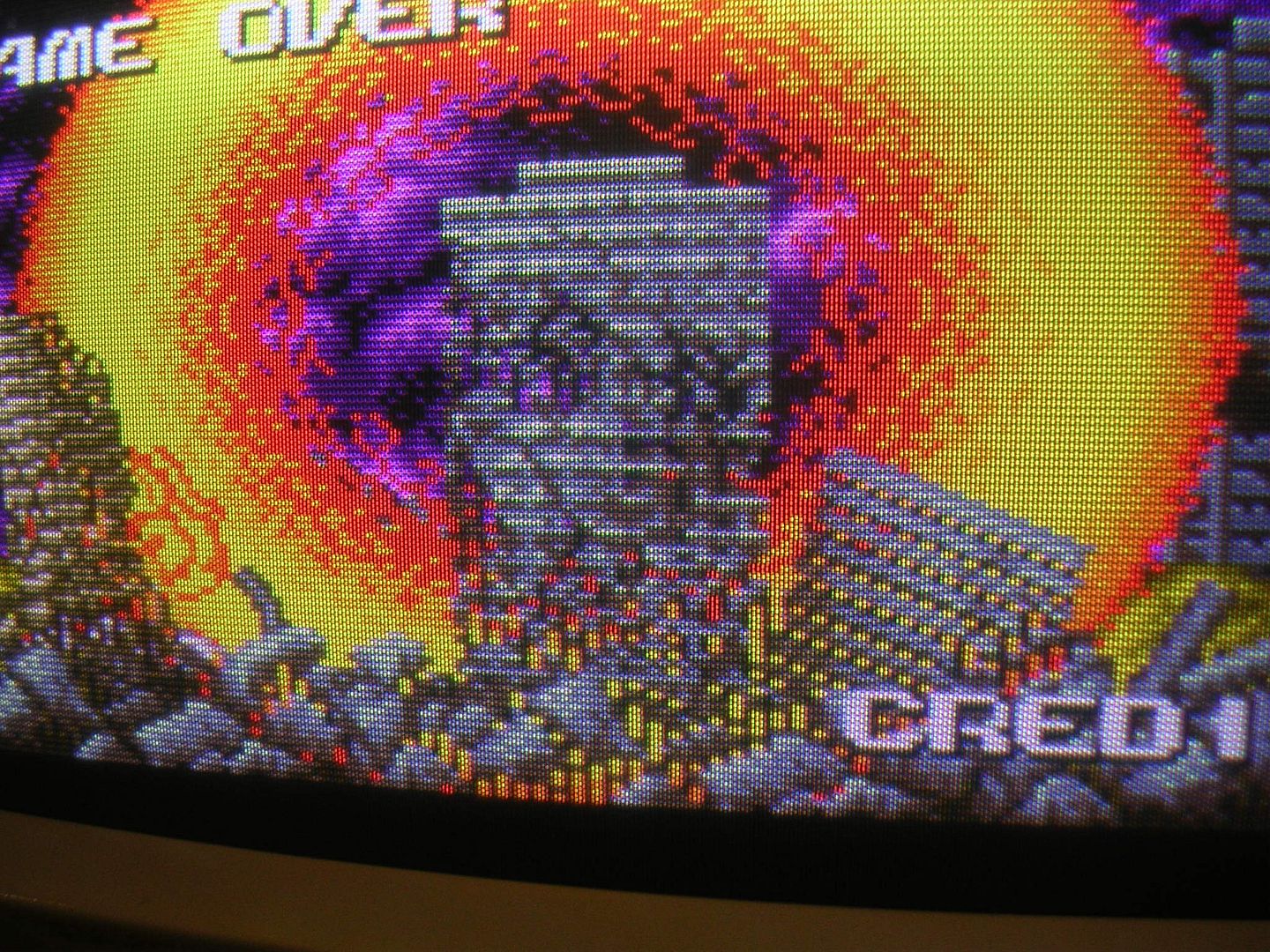
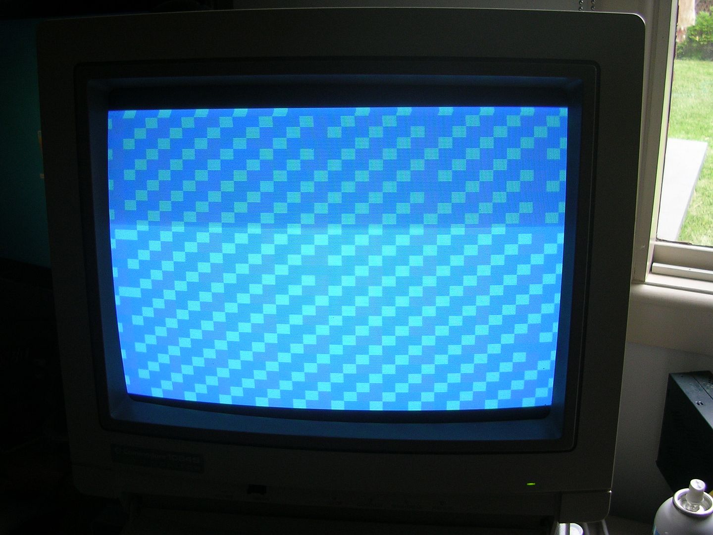
Another change was that every so often the screen would now flash up blue zig zag patterns, clearly it was still crashing, but something had changed.
As I was sttill looking for something nasty on the main CPU buses, and with the constant shifting sand of faults on PCB#1 fresh in my mind, I hooked up the Fluke and re-ran the RAM and ROM tests, which it still passed, but with a CPU in the socket the board stayed resolutely dead.
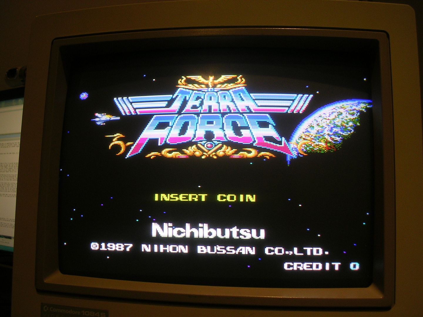
You can actually use the CPU in the Fluke pod as a normal CPU and get it to try to run the board with the "Run UUT" button, UUT being "Unit Under Test". I had had no luck with a real 68000 CPU but the fluke is easier to reset rapidly as you don't need to constantly flick the power to reset the board. I tried to reset the board and issued the Run UUT command with a start address of 0x0 and the first 3 times I got no response, but on the fourth time it booted up and the board ran and stayed running.
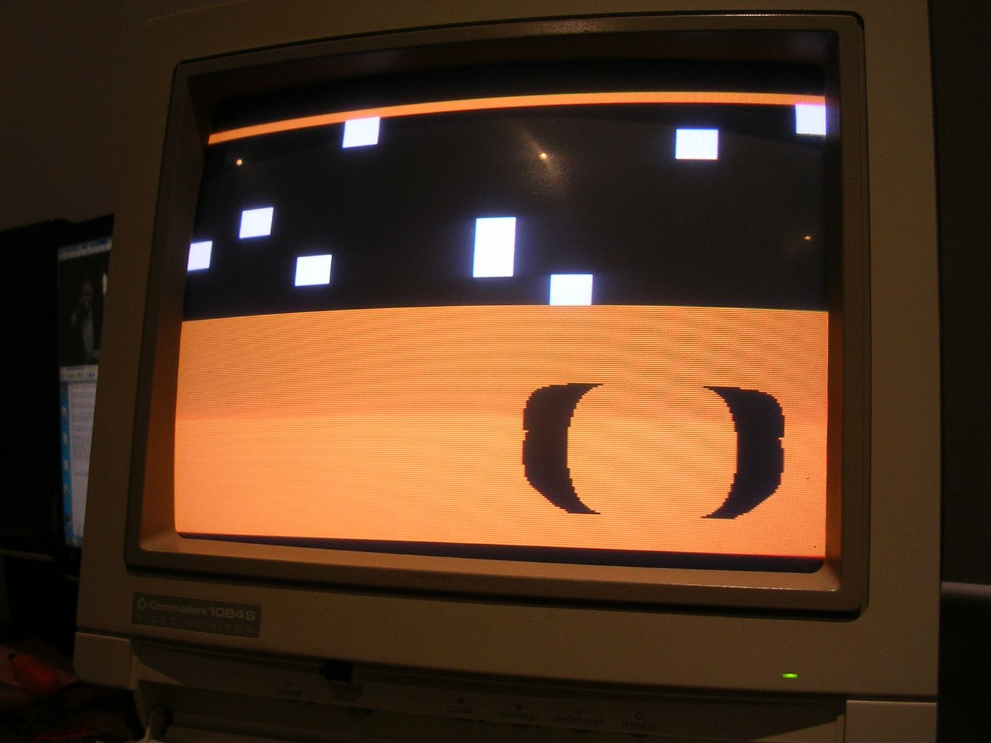
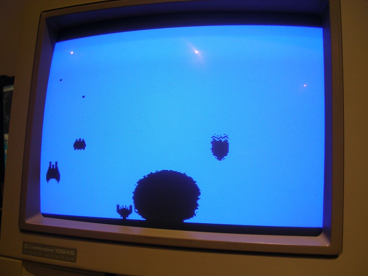
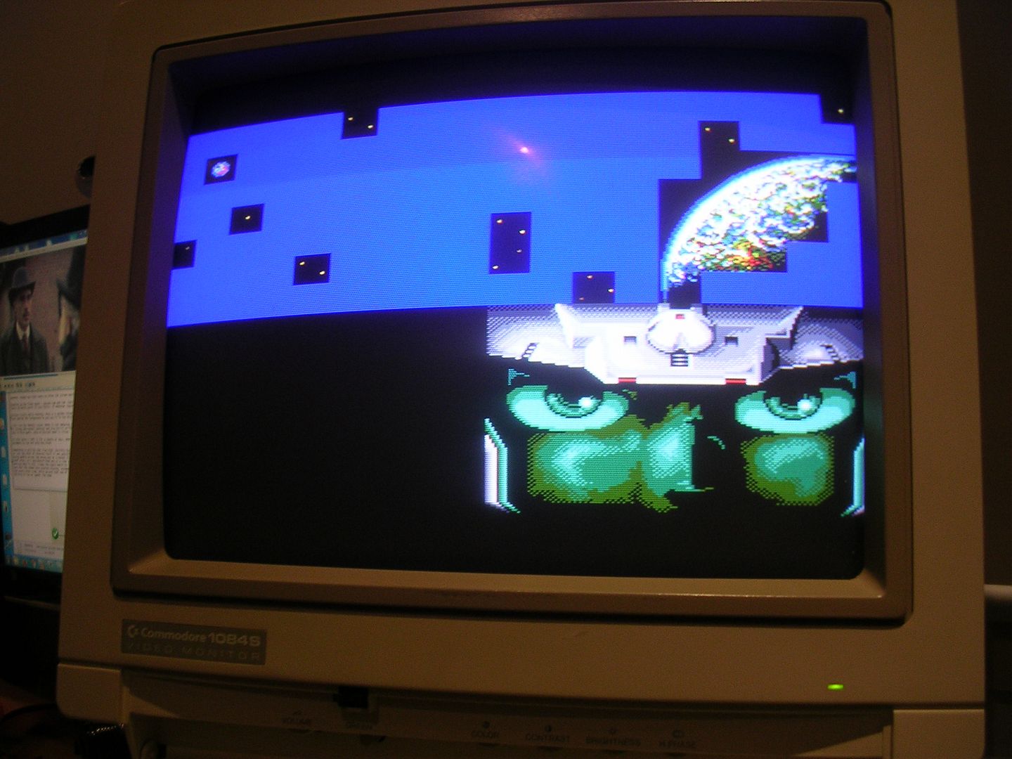
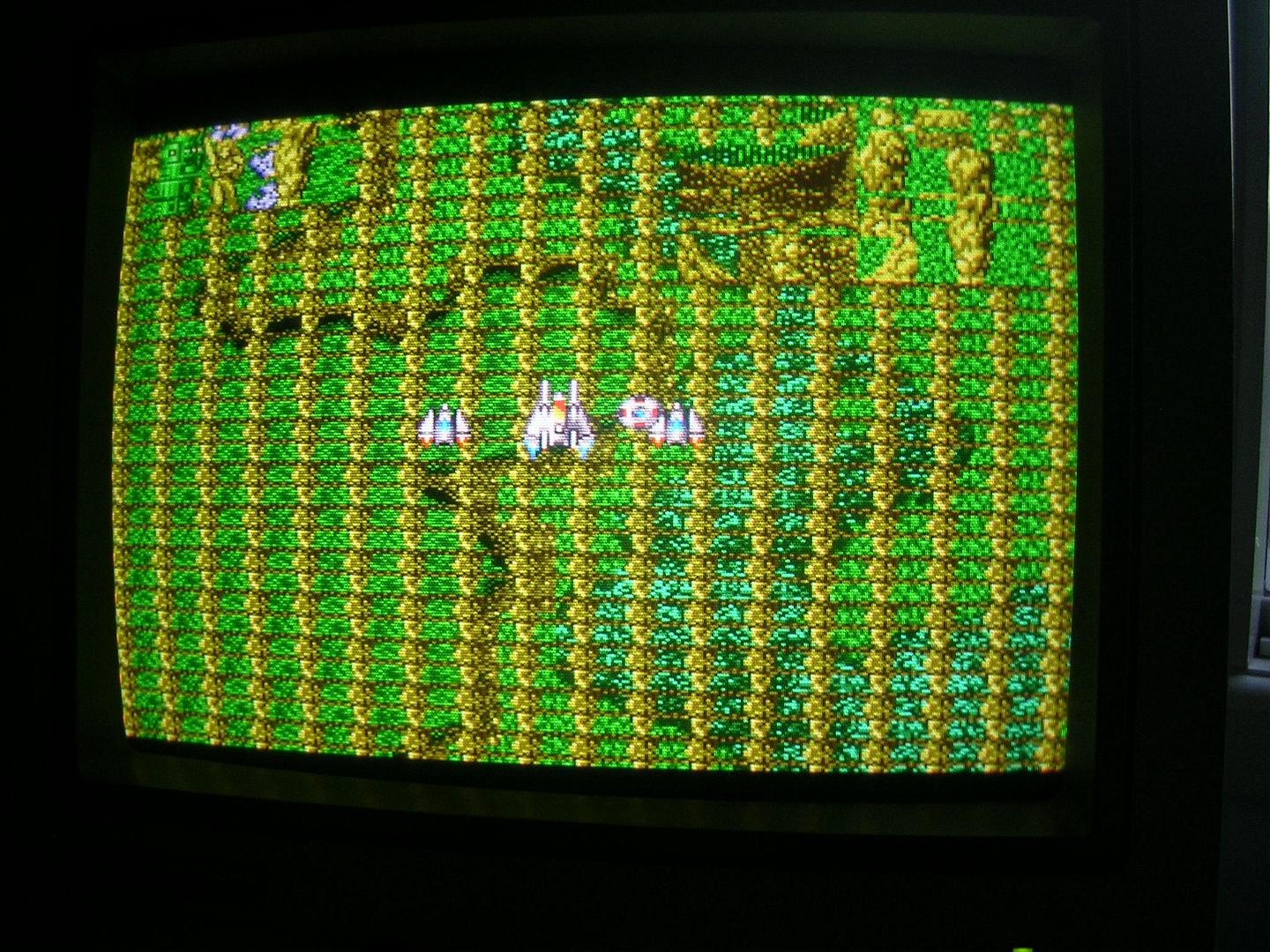
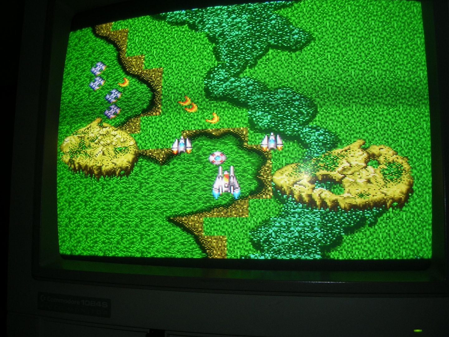
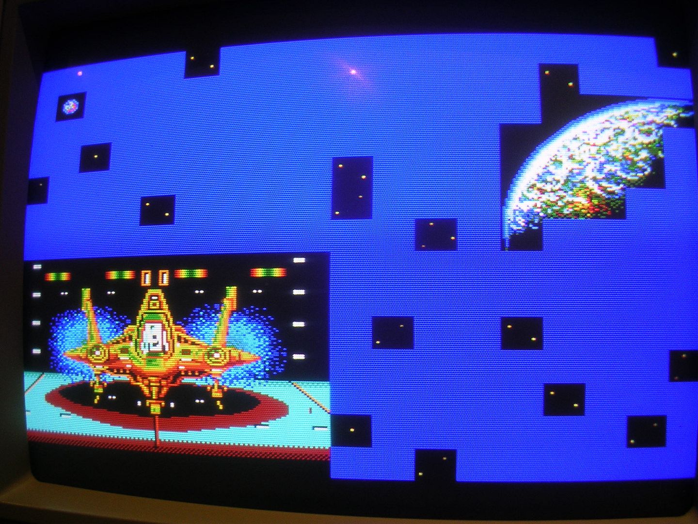
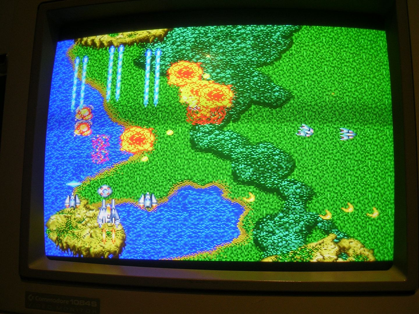
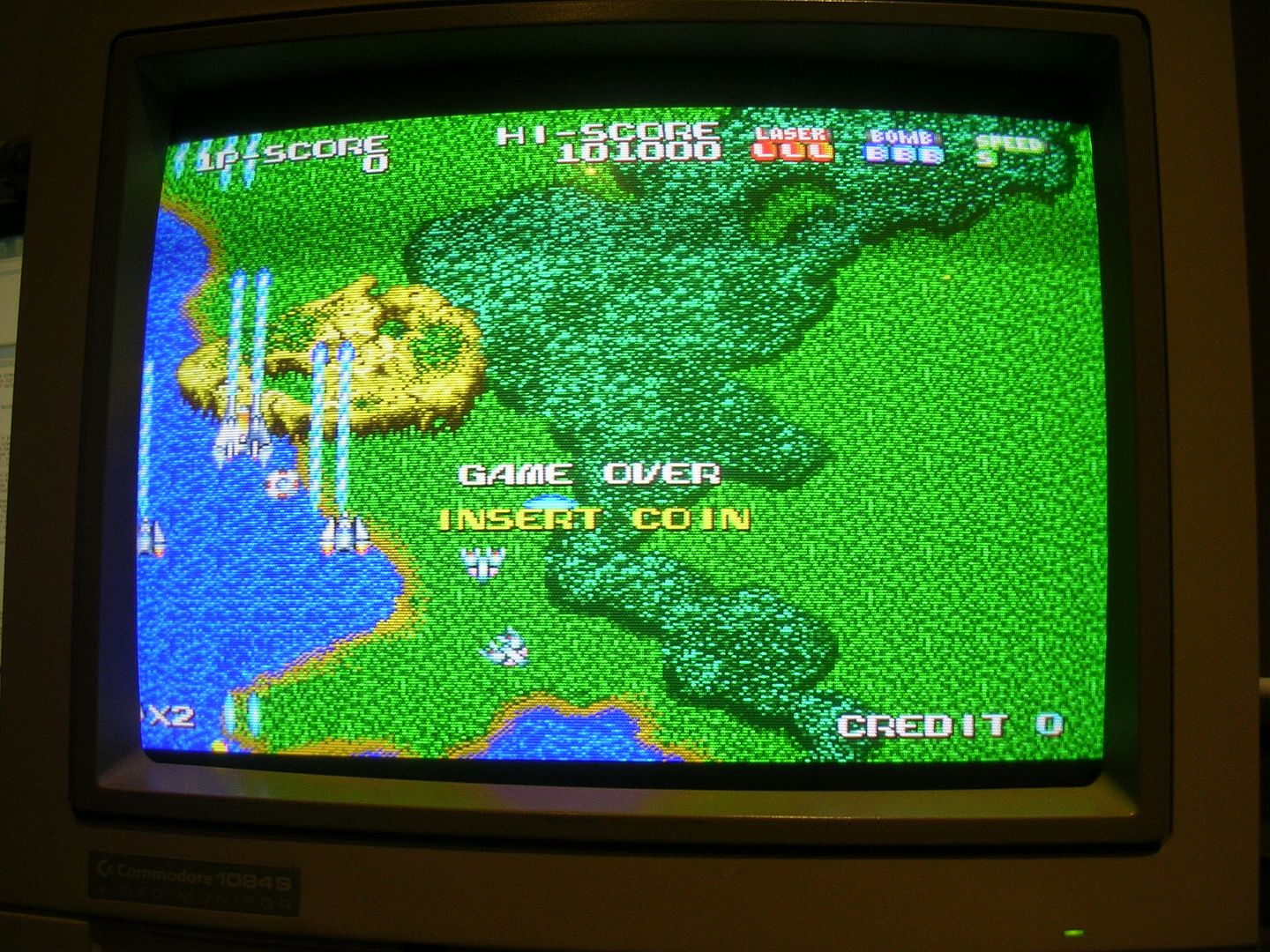
The board had weird faults while running, there were B's everywhere...
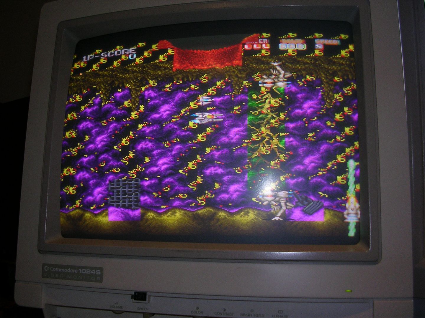
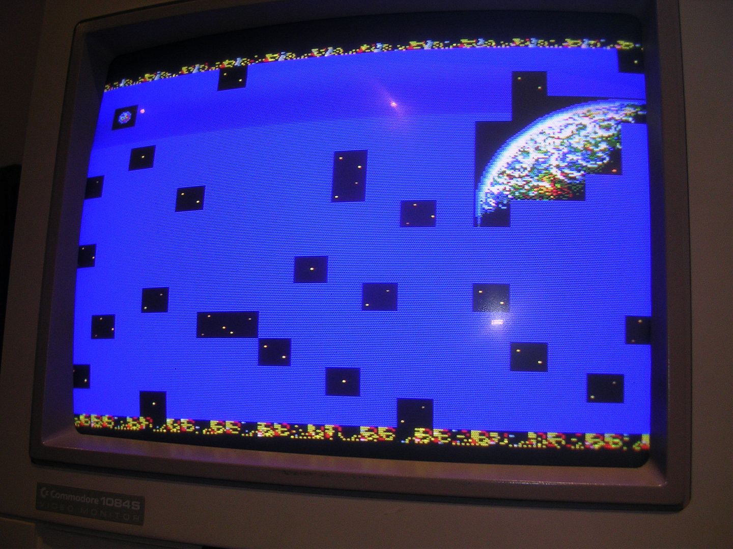
the ship in the intro was a golden colour rather than silver...
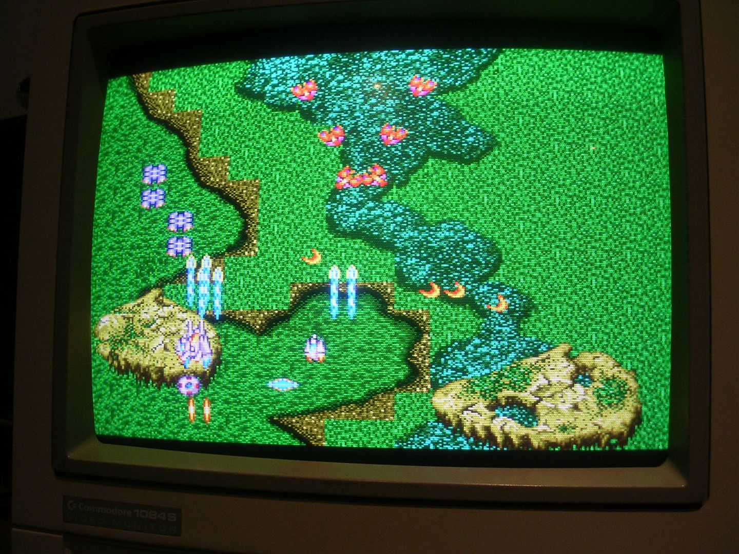
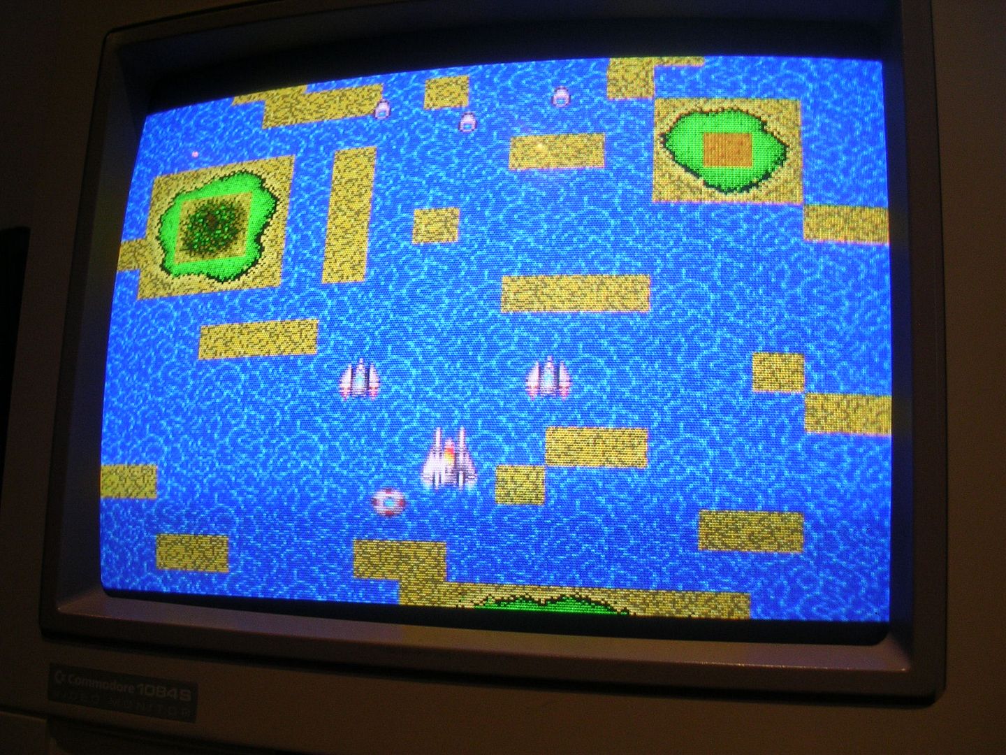
... the sea was the same colour as the land...
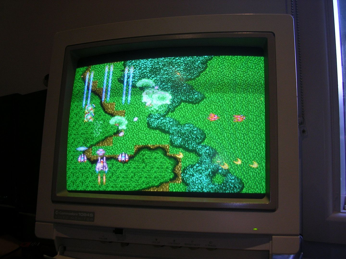
...and there were blocky halos around some features.
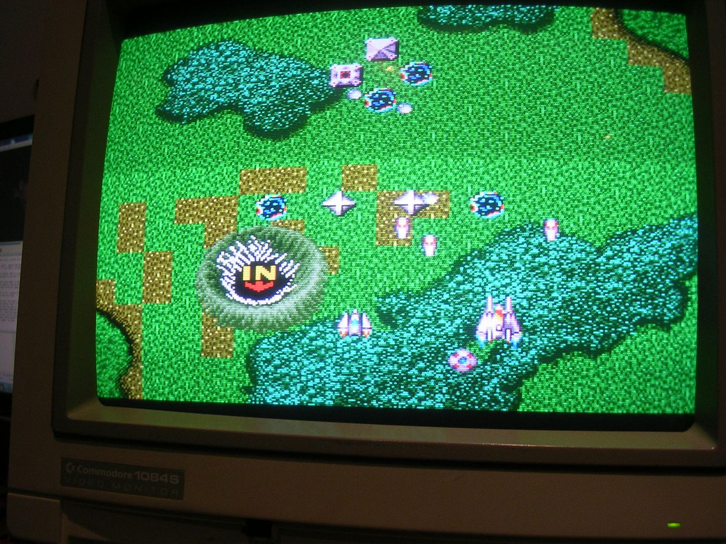
Also the priority system has the text behind the foreground so you see it in the distance between the trees on the forest level in attract mode.
Part 2 coming soon...