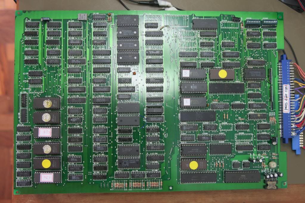
here is the picture from my bubble bobble single board:
http://www.directupload.net/file/d/3198 ... xj_jpg.htm
it has more roms than your board !?
i change alredy the roms but the fault is still there.
The treasure room is still not working fine
simon
Bubble Bobble Bootleg info
-
golani

- Posts: 50
- Joined: October 20th, 2011, 2:36 pm
- Location: Austria
Re: Bubble Bobble Bootleg info
Last edited by golani on December 6th, 2015, 11:47 pm, edited 2 times in total.
-
joaoljr

- Please Continue...
- Posts: 145
- Joined: September 25th, 2012, 3:22 am
- Location: Brazil
Re: Bubble Bobble Bootleg info
My board has the same number of ROMs, but it looks quite different:golani wrote: it has more roms than your board !?
Just to confirm, you tried to replace the 27256 ROMs at position N2 and S2 with a pair of 27512, right?golani wrote: i change alredy the roms but the fault is still there.
The treasure room is still not working fine
The treasure room fault in my board also looked very different:
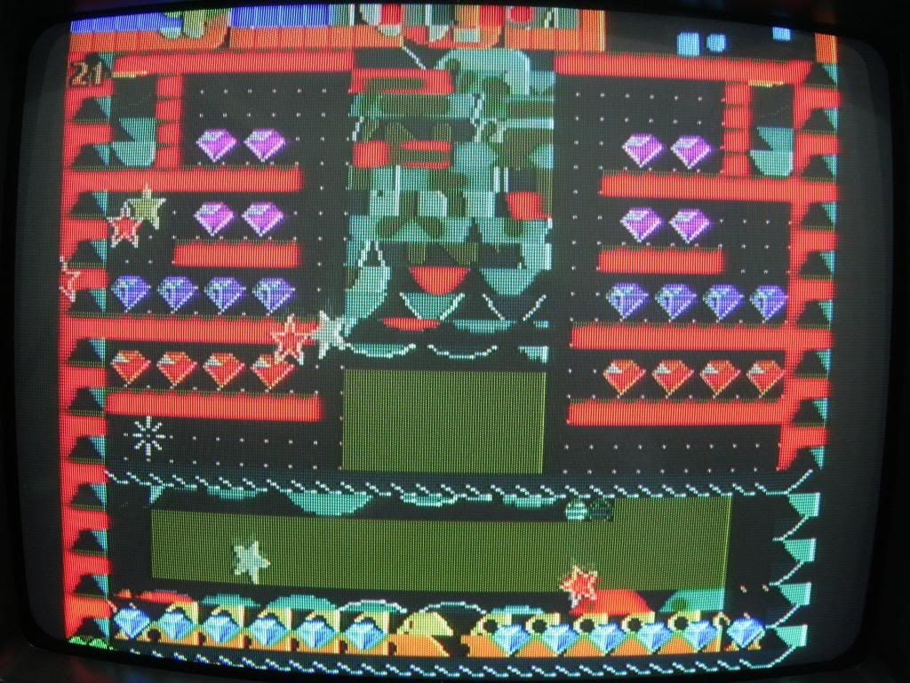
It seems in your board the graphic circuit is reading the same value, since you have a plain background image.
Either your new ROMs have 0x00 / 0xFF at the lower half or the ROM selection circuit is not selecting that address range.
You need to provide more details:
- For the ROM at position S2, where are the pins 1 and 20 connected to?
- For the 74LS138 at position G4, where is the pin 13 connected to?
- Were the new images correctly flashed with 64K bytes of data each (address range 0000 to FFFF)?
Punji
-
golani
- Posts: 50
- Joined: October 20th, 2011, 2:36 pm
- Location: Austria
Re: Bubble Bobble Bootleg info
the new images where correctly flashed
74LS138 at position G4, the pin 13,14 and 15 ending on the pcb.
there is nothing connected-
image look to the red circle:
http://s1.directupload.net/file/d/3198/5rmfluya_jpg.htm"
this kind of pcb has also another fault:
the final enemy is a block:
http://s14.directupload.net/file/d/3198 ... nj_jpg.htm"
simon
Last edited by golani on December 6th, 2015, 11:48 pm, edited 1 time in total.
-
joaoljr
- Please Continue...
- Posts: 145
- Joined: September 25th, 2012, 3:22 am
- Location: Brazil
Re: Bubble Bobble Bootleg info
Simon, also please remove ROMs at positions N2 and S2 and take a picture from inside the sockets.
From what I gathered so far, pin 20 on these two ROMs are connected to pin 10 on the 74LS138 (signal C5).
That, plus the fact that pin 1 on the ROMs is connected to VCC, means that only 32K will ever get selected,
i.e., the upper half of the 27512. Any access to the lower half will read a floating bus value (likely 0x00 / 0xFF),
which seems consistent with the treasure room picture. You can't fix the issue unless you cut some traces and
modify the selection circuit. We would need to know where pin 20 of the other four ROMs (H2 / L2 and P2 / Q2)
are connected to in order to figure out how to do that.
I did not check the boss level yet to confirm which graphics address range it is using.
Punji
-
golani
- Posts: 50
- Joined: October 20th, 2011, 2:36 pm
- Location: Austria
Re: Bubble Bobble Bootleg info
picture from inside the sockets N2 and S2 :
http://s14.directupload.net/file/d/3199 ... no_jpg.htm"
your right pin 20 on these two ROMs are connected to pin 10 on the 74LS138
pin 20 of the other four ROMs (H2 / L2 and P2 / Q2)
are connected to pin 3 on the 74LS138 at position G4
simon
http://s14.directupload.net/file/d/3199 ... no_jpg.htm"
your right pin 20 on these two ROMs are connected to pin 10 on the 74LS138
pin 20 of the other four ROMs (H2 / L2 and P2 / Q2)
are connected to pin 3 on the 74LS138 at position G4
simon
-
joaoljr
- Please Continue...
- Posts: 145
- Joined: September 25th, 2012, 3:22 am
- Location: Brazil
Re: Bubble Bobble Bootleg info
I confirmed that the boss graphics are stored at the same ROM range as the treasure room.joaoljr wrote:I did not check the boss level yet to confirm which graphics address range it is using.
I also verified on my single board after replacing the ROMs and the boss is displayed just fine.
Punji
-
joaoljr
- Please Continue...
- Posts: 145
- Joined: September 25th, 2012, 3:22 am
- Location: Brazil
Re: Bubble Bobble Bootleg info
So, if these four ROMs are being selected by that same signal, it means something else is controlling the output enable of each pair.golani wrote: pin 20 of the other four ROMs (H2 / L2 and P2 / Q2)
are connected to pin 3 on the 74LS138 at position G4
Anyway, that should not matter. I will post instructions on how to fix the selection circuit.
Punji
-
golani
- Posts: 50
- Joined: October 20th, 2011, 2:36 pm
- Location: Austria
Re: Bubble Bobble Bootleg info
(N2 and S2 ROMs pin 22 is connected to ground)
pin 22 from H2 and P2 goes to 74LS04 pin 13 at position B2
pin 22 from L2 and Q2 goes to 74LS04 pin 12 at position B2
simon
pin 22 from H2 and P2 goes to 74LS04 pin 13 at position B2
pin 22 from L2 and Q2 goes to 74LS04 pin 12 at position B2
simon
-
joaoljr
- Please Continue...
- Posts: 145
- Joined: September 25th, 2012, 3:22 am
- Location: Brazil
Re: Bubble Bobble Bootleg info
Simon, please follow the six steps below to change the ROM selection circuit in order to try to fix your graphics issue.
Note that RED means "cut trace" and BLUE means "solder wire".
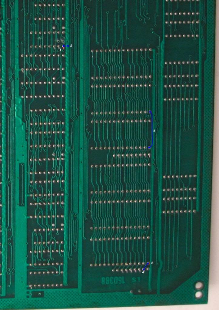
1- Cut the trace that goes from the via to pin 1 on the 74LS138 at position G4. Use a sharp knife and a steady hand!
2- Connect pin 1 on the 74LS138 at position G4 to VCC (gently scrap the mask above the trace). This will allow the lower half of 27512 to be selected.
3- Cut the trace that goes from pin 1 on the ROM at position S2 to VCC.
4- Connect pin 1 on the ROM at position S2 to pull-up resistor of address line CA15. This will enable full 64K address for 27512.
5- Connect pin 1 on the ROM at position N2 to pin 1 of the ROM at position M2. This will enable full 64K address for 27512.

6- Cut the trace that goes from VCC to pin 1 of the ROM at position N2.
Punji
Note that RED means "cut trace" and BLUE means "solder wire".
1- Cut the trace that goes from the via to pin 1 on the 74LS138 at position G4. Use a sharp knife and a steady hand!
2- Connect pin 1 on the 74LS138 at position G4 to VCC (gently scrap the mask above the trace). This will allow the lower half of 27512 to be selected.
3- Cut the trace that goes from pin 1 on the ROM at position S2 to VCC.
4- Connect pin 1 on the ROM at position S2 to pull-up resistor of address line CA15. This will enable full 64K address for 27512.
5- Connect pin 1 on the ROM at position N2 to pin 1 of the ROM at position M2. This will enable full 64K address for 27512.
6- Cut the trace that goes from VCC to pin 1 of the ROM at position N2.
Punji
-
golani
- Posts: 50
- Joined: October 20th, 2011, 2:36 pm
- Location: Austria
Re: Bubble Bobble Bootleg info
hello,
i do so you show me.
i got now bad picture at gameplay.
http://s14.directupload.net/file/d/3199 ... on_jpg.htm"
http://s1.directupload.net/file/d/3199/2nyh8d8o_jpg.htm"
i think there is something going wrong.
simon
i do so you show me.
i got now bad picture at gameplay.
http://s14.directupload.net/file/d/3199 ... on_jpg.htm"
http://s1.directupload.net/file/d/3199/2nyh8d8o_jpg.htm"
i think there is something going wrong.
simon
Last edited by golani on December 6th, 2015, 11:49 pm, edited 1 time in total.
-
joaoljr
- Please Continue...
- Posts: 145
- Joined: September 25th, 2012, 3:22 am
- Location: Brazil
Re: Bubble Bobble Bootleg info
Yes, but note that +5V is coming from a pull-up resistor network at position T2, not true VCC.golani wrote:i have now still at this pins +5volt (vcc)
on all 6 roms at pin 1 and 28
is that right?
These pins should still be able to switch to 0V, depending on the state of address line CA15.
You may verify that with an oscilloscope, if you have one.
Or turn off the board and check the resistance with a multimeter from any ROM pin 1 to +5 supply line.
It should be a few K ohms. If it is close to 0 ohms then you have not cut the traces properly
(and that for sure will cause some weird graphic issues like the screenshots you posted).
Could you please post some pictures of the modified board?
Also, please confirm to me where pin 1 of the 74LS138 was connected to before you cut the trace to it.
Punji
-
golani
- Posts: 50
- Joined: October 20th, 2011, 2:36 pm
- Location: Austria
Re: Bubble Bobble Bootleg info
sorry i dont own an oscilloscope
pin 1 of the 74LS138 was connected before to the roms pin 1 and to an 74LS37N4 pin15 at position H6
i check the resistance from any ROM pin 1 to +5 supply line
thats the problem: i have on all 6 roms almost 0 ohm
i see now there is also a trace from pin 1 of the 74LS138 to the roms pin 1- i cut it but nothing change.
now i restore the board to the original back and there is an fault.
i think i have destroyed a chip.
i miss now one colour - no green bubbles!?
and the picture is almost red.
http://s7.directupload.net/file/d/3200/em378wz3_jpg.htm"
http://s7.directupload.net/file/d/3200/fa3gorog_jpg.htm"
simon
Last edited by golani on December 6th, 2015, 11:51 pm, edited 1 time in total.
-
joaoljr
- Please Continue...
- Posts: 145
- Joined: September 25th, 2012, 3:22 am
- Location: Brazil
Re: Bubble Bobble Bootleg info
Simon, the 0 ohms problem could be caused by pin 1 of ROM at position N2. The socket covers the board,
we don't know what is below its left side. Maybe there is a trace connecting pin 1 to pin 28, so VCC could still be coming from there.
Can you try to verify if that was the problem?
I think you should give it another try... I'm pretty confidente that we will be able to fix the treasure room and boss graphics issue with these changes.
I tried to reproduce the green color issue by disabling one of the ROMs but could not. Are you sure you have the GREEN signal properly connected to your monitor?
I see something strange near pin 28 of ROM at position S2. Is that trace cut?
Punji
-
golani
- Posts: 50
- Joined: October 20th, 2011, 2:36 pm
- Location: Austria
Re: Bubble Bobble Bootleg info
the 0 ohm problem was there because it is still a connection to pin 1 of ROM at position N2 - i cut it now i have 35 ohm
http://s7.directupload.net/file/d/3200/q4o4cy7i_jpg.htm"
near pin 28 of ROM at position S2. that trace is not cut (goes to S2 pin20)
simon
http://s7.directupload.net/file/d/3200/q4o4cy7i_jpg.htm"
near pin 28 of ROM at position S2. that trace is not cut (goes to S2 pin20)
simon
-
joaoljr
- Please Continue...
- Posts: 145
- Joined: September 25th, 2012, 3:22 am
- Location: Brazil
Re: Bubble Bobble Bootleg info
I'm confused. You cut that trace near the 74LS138 that you indicated in the picture? This trace should be going to CA15 address line, not VCC. Also, 35 ohms seems too little. You should have at least a few K ohms.golani wrote:the 0 ohm problem was there because it is still a connection to pin 1 of ROM at position N2 - i cut it now i have 35 ohm
The best is to remove the jumpers from steps 3 and 5, after you cut the traces, and measure the resistance from pin 1 to VCC on both ROMs at position S2 and N2. It should read as unconnected (infinite ohms).
Punji
-
golani
- Posts: 50
- Joined: October 20th, 2011, 2:36 pm
- Location: Austria
Re: Bubble Bobble Bootleg info
i cut that trace near the 74LS138 because its going right to pin 1 of ROM at position N2 .
it makes a short-circuit before.
i cut before only on bottom side 74LS138 pin1 as you pictured.
thats the reason the board did not works?
simon
it makes a short-circuit before.
i cut before only on bottom side 74LS138 pin1 as you pictured.
thats the reason the board did not works?
simon
-
golani
- Posts: 50
- Joined: October 20th, 2011, 2:36 pm
- Location: Austria
Re: Bubble Bobble Bootleg info
i remove the jumpers from steps 3 and 5 -
after i measure the resistance from pin 1 to VCC on both ROMs at position S2 and N2.
It has 10 k ohm .
after connecting one of the bridge i has around 30 ohm.
simon
after i measure the resistance from pin 1 to VCC on both ROMs at position S2 and N2.
It has 10 k ohm .
after connecting one of the bridge i has around 30 ohm.
simon
-
joaoljr
- Please Continue...
- Posts: 145
- Joined: September 25th, 2012, 3:22 am
- Location: Brazil
Re: Bubble Bobble Bootleg info
Ok, I understand now. You are right, it is also necessary to cut the trace at the top of the board that goes to pin 1 on the 74LS138,golani wrote: i cut that trace near the 74LS138 because its going right to pin 1 of ROM at position N2 .
it makes a short-circuit before.
i cut before only on bottom side 74LS138 pin1 as you pictured.
like you did. BUT you also need to re-connected the previous address signal to pin 1 of all six ROMs, like in the picture below:

Sorry, you should remove jumpers from steps 4 and 5, not 3. You got 10 k ohms, so I believe you still had jumper 4 connected to the pull-up resistor. If that was the case then I think we are good.golani wrote: i remove the jumpers from steps 3 and 5 -
after i measure the resistance from pin 1 to VCC on both ROMs at position S2 and N2.
It has 10 k ohm .
after connecting one of the bridge i has around 30 ohm.
Punji
-
lucusam
- Please Continue...
- Posts: 2
- Joined: March 21st, 2013, 9:52 am
- Location:
Re: Bubble Bobble Bootleg info
Thanks for all of your hard work.
I can't wait to patch my bootleg board with this version. I'm still waiting for my board to arrive, in the meantime
I have been testing out your patch with sboblbob ( set 2 ) in MAME.
I have noticed the game will reset. I don't know if this will work on the actual hardware just yet. Not being
familiar with the games architecture but it seems like the watchdog is waiting for something, still haven't
had a chance to debug yet & not too familiar with Z80.
I have been able to reproduce the problem by doing the following steps.
* Insert 1 credit and play the game for awhile
* Enter your high score
* Allow game to enter attract mode
Game should reset, if it doesn't then try insert a credit and start a game.
I have been able to reproduce this quite easily. Curious to see if anybody can reproduce this on the various bootlegs in existence.
-
ninn

- TheRedKnight's Lover
- Posts: 934
- Joined: September 5th, 2011, 1:24 pm
- Location: Vienna, Austria, Europe
- eBay: 8bitbitch
Re: Bubble Bobble Bootleg info
as far as i know, game writes the highscores not immediately, probably while the attractmode. did you hack the new traces / ATMEL-Chip-Adapter into your mame too? Or did you tested roms without the highscore-hack?