Hi.
I'm helping out a friend with a Video RAM replacement.. Well actually, a previus owner had pulled out the RAM so I need to totally rewire the ram.
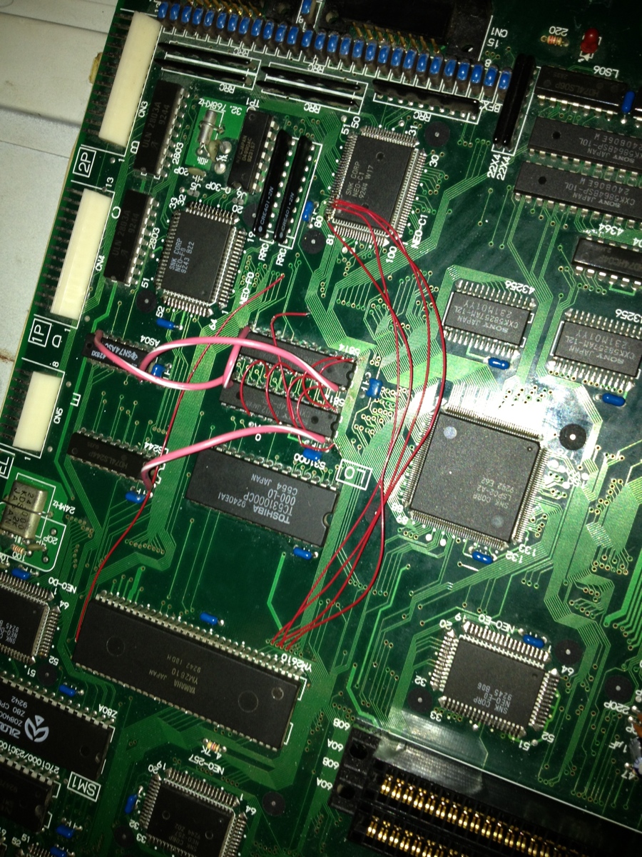
I've managed to replace all "visible" trace with thin red wire but I still get Video 8000 0000 0100.. So i'm guessing theres some hidden traces to some of the "empty" pins..
This is what we had to start with..
MVS Schematics for massive trace issue? WORKS!
-
KmanSweden

- KmanSweden
- Posts: 1242
- Joined: October 13th, 2010, 10:37 am
- Location: Stockholm, Sweden
- eBay: KmanSweden
- Initials: PKK
- Contact:
MVS Schematics for massive trace issue? WORKS!
You do not have the required permissions to view the files attached to this post.
Last edited by KmanSweden on April 21st, 2013, 5:43 pm, edited 2 times in total.
Up the Irons!
-
Rossyra

- Supermod
- Posts: 7902
- Joined: February 12th, 2009, 1:24 am
- Location: UK
-
KmanSweden
- KmanSweden
- Posts: 1242
- Joined: October 13th, 2010, 10:37 am
- Location: Stockholm, Sweden
- eBay: KmanSweden
- Initials: PKK
- Contact:
Re: MVS Schematics?
Not in my Pdf. I'll dig out my paper one and have a look.
Edit: nope..
Edit: nope..
Up the Irons!
-
KmanSweden
- KmanSweden
- Posts: 1242
- Joined: October 13th, 2010, 10:37 am
- Location: Stockholm, Sweden
- eBay: KmanSweden
- Initials: PKK
- Contact:
Re: MVS Schematics?
Thanks!Rossyra wrote:http://wiki.neogeodev.org/index.php?tit ... schematics
Up the Irons!
-
leonardoliveira

- Please Continue...
- Posts: 692
- Joined: August 30th, 2012, 5:53 am
- Location: Brazil
- Initials: leo
Re: MVS Schematics?
KmanSweden wrote:Hi.
I'm helping out a friend with a Video RAM replacement.. Well actually, a previus owner had pulled out the RAM so I need to totally rewire the ram.
I've managed to replace all "visible" trace with thin red wire but I still get Video 8000 0000 0100.. So i'm guessing theres some hidden traces to some of the "empty" pins..
This is what we had to start with..
By looking at that picture and what bit the BIOS reports as bad I can even tell you which trace is bad without a schematic ...
Horrible damage btw !
Try pin 11 of the chip which is closer to the viewer.

-
KmanSweden
- KmanSweden
- Posts: 1242
- Joined: October 13th, 2010, 10:37 am
- Location: Stockholm, Sweden
- eBay: KmanSweden
- Initials: PKK
- Contact:
Re: MVS Schematics?
Cool. Try it how?leonardoliveira wrote:
By looking at that picture and what bit the BIOS reports as bad I can even tell you which trace is bad without a schematic ...
Horrible damage btw !
Try pin 11 of the chip which is closer to the viewer.
Up the Irons!
-
KmanSweden
- KmanSweden
- Posts: 1242
- Joined: October 13th, 2010, 10:37 am
- Location: Stockholm, Sweden
- eBay: KmanSweden
- Initials: PKK
- Contact:
-
leonardoliveira
- Please Continue...
- Posts: 692
- Joined: August 30th, 2012, 5:53 am
- Location: Brazil
- Initials: leo
-
Rossyra
- Supermod
- Posts: 7902
- Joined: February 12th, 2009, 1:24 am
- Location: UK
Re: MVS Schematics?
There's your problem right there.
It's the red weed from War of the Worlds.
In all seriousness, these boards can end up totally goosed from a battery leak, has that happened here by any chance? Just wondering because I have one that looks like that and I've never got to the bottom of it yet. It's turning into my life's project.
What board is it? Did the previous owner butcher it for the RAM only, or was he actually trying to fix it?

-
KmanSweden
- KmanSweden
- Posts: 1242
- Joined: October 13th, 2010, 10:37 am
- Location: Stockholm, Sweden
- eBay: KmanSweden
- Initials: PKK
- Contact:
Re: MVS Schematics?
God morning, Gents.
It's NeoGeo 2-slot mobo I'm trying to fix for a friend. It was missing the RAM's completely and there was massive trace damage in and around where the RAM's used to be.
I got the board, new RAM and a prayer from my friend. We're not going for pretty here. We're aiming for "It's Alive!!!"
I got to 8000 5555 55FE or something before I realized that they didn't even get +5v because the traces are so **** up (hence the big pink wires).
I'll try looking at the schematics again today, hoping Leo will pop back in with a clarification about PIn 11..
Up the Irons!
-
Hewitson

- Please Continue...
- Posts: 558
- Joined: June 4th, 2011, 8:59 am
- Location: Melbourne, Australia
- Initials: BJA
Re: MVS Schematics for massive trace issue?
Wow.. What was the ram desoldered with? A blowtorch?
crunchywasp wrote:During your visit you could reverse his evil honey trap and tell him you're a bit uncertain about spending an hour inside his box
-
KmanSweden
- KmanSweden
- Posts: 1242
- Joined: October 13th, 2010, 10:37 am
- Location: Stockholm, Sweden
- eBay: KmanSweden
- Initials: PKK
- Contact:
Re: MVS Schematics for massive trace issue?
Hewitson wrote:Wow.. What was the ram desoldered with? A blowtorch?
Up the Irons!
-
leonardoliveira
- Please Continue...
- Posts: 692
- Joined: August 30th, 2012, 5:53 am
- Location: Brazil
- Initials: leo
Re: MVS Schematics for massive trace issue?
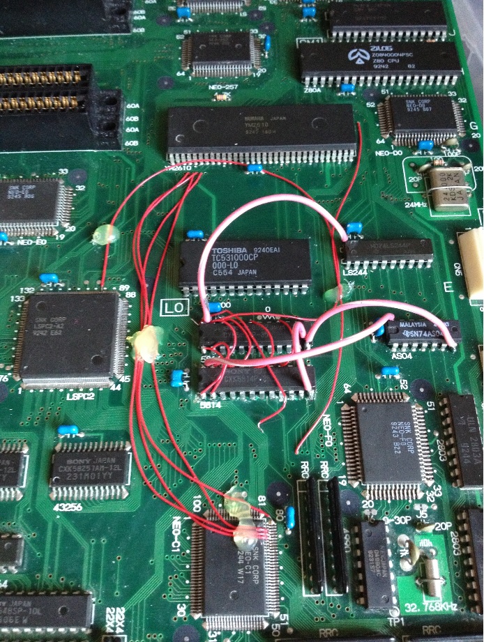
Well, this a breakdown of what the NEO GEO BIOS is trying to tell you:
ADDRESS Written READ
8000 5555 55FE
So now you're worse now than when you had 8000 0000 0100. That means the lower SRAM chip probably didn't even receive any control strobe.
It's important to keep in mind that for a successful write the RAM chip require a certain configuration on the pins. Also for read another configuration is required:

For a write, pins /CS (Chip Select or /CE Chip Enable enables the core of the chip for access). The chip will be ready but will only accept a write after an low pulse is applied also to /WE (Write Enable).
For a read, you want to pulse pins /CS and /OE (output enable).
On the use given for the chips on the NEO GEO, the chips are aways enabled. Since the RAMs are not in a bus, but connected straight to the LSPC chip, the /CS and /OE pins are tied straight to GND (meaning the chips will be aways active and on read mode). Setting /WE low causes the chip to enter on write mode regardless of the state of /OE pin. SNK exploited that behavior to simplify the circuit and save one pin on the LSPC chip. So make sure pins 18 and 20 on both chips are connected to GND... Also very important that pin 21 is tied on the two chips and connected to LSPC-A2 pin 86. That's the write strobe.
Since the chips are 8 bit, you need two to form the 16 bit bank the LSPC chip need. Address lines (C0-C10 and the CWE write control strobe are tied together on the two RAM chips).
This memory bank in particular is used by the LSPC chip to draw the stripes which form the playfield (Aka everything that is not FIX) which is basically where the game graphical action happens.
So as reference use the LSPC-A2 pinout:
http://wiki.neogeodev.org/index.php?title=LSPC2-A2"
The fast SRAM is connected to it as "VRAM Bank 1".
Make sure all traces to to each chip (SRAMS and LSPC) are alright.
ADDRESS Written READ
8000 5555 55FE
So now you're worse now than when you had 8000 0000 0100. That means the lower SRAM chip probably didn't even receive any control strobe.
It's important to keep in mind that for a successful write the RAM chip require a certain configuration on the pins. Also for read another configuration is required:
For a write, pins /CS (Chip Select or /CE Chip Enable enables the core of the chip for access). The chip will be ready but will only accept a write after an low pulse is applied also to /WE (Write Enable).
For a read, you want to pulse pins /CS and /OE (output enable).
On the use given for the chips on the NEO GEO, the chips are aways enabled. Since the RAMs are not in a bus, but connected straight to the LSPC chip, the /CS and /OE pins are tied straight to GND (meaning the chips will be aways active and on read mode). Setting /WE low causes the chip to enter on write mode regardless of the state of /OE pin. SNK exploited that behavior to simplify the circuit and save one pin on the LSPC chip. So make sure pins 18 and 20 on both chips are connected to GND... Also very important that pin 21 is tied on the two chips and connected to LSPC-A2 pin 86. That's the write strobe.
Since the chips are 8 bit, you need two to form the 16 bit bank the LSPC chip need. Address lines (C0-C10 and the CWE write control strobe are tied together on the two RAM chips).
This memory bank in particular is used by the LSPC chip to draw the stripes which form the playfield (Aka everything that is not FIX) which is basically where the game graphical action happens.
So as reference use the LSPC-A2 pinout:
http://wiki.neogeodev.org/index.php?title=LSPC2-A2"
The fast SRAM is connected to it as "VRAM Bank 1".
Make sure all traces to to each chip (SRAMS and LSPC) are alright.
-
KmanSweden
- KmanSweden
- Posts: 1242
- Joined: October 13th, 2010, 10:37 am
- Location: Stockholm, Sweden
- eBay: KmanSweden
- Initials: PKK
- Contact:
Re: MVS Schematics for massive trace issue?
No,no, no. I have 8000 0000 0100 now. I had 8000 5555 55FE before hooking up the 5v ang GND (big pink wires).leonardoliveira wrote:So now you're worse now than when you had 8000 0000 0100.
Thanks for the write up.
So 1.) I'll check grounding on pins 18 and 20. (x2)
2.) Check continouty (spelled the crap out of that word..) from pin 21's to LSPC-A2 pin 86. (x2)
3.) Probe CS, WE and OE for signals.. (x2)
Cheers.
Up the Irons!
-
leonardoliveira
- Please Continue...
- Posts: 692
- Joined: August 30th, 2012, 5:53 am
- Location: Brazil
- Initials: leo
Re: MVS Schematics for massive trace issue?
CS and OE are tied to GND so there won't be any signal on them.KmanSweden wrote:No,no, no. I have 8000 0000 0100 now. I had 8000 5555 55FE before hooking up the 5v ang GND (big pink wires).leonardoliveira wrote:So now you're worse now than when you had 8000 0000 0100.
Thanks for the write up.
So 1.) I'll check grounding on pins 18 and 20. (x2)
2.) Check continouty (spelled the crap out of that word..) from pin 21's to LSPC-A2 pin 86. (x2)
3.) Probe CS, WE and OE for signals.. (x2)
Cheers.
All Axx pins are connected together on both chips and then go to LSPC2-A2. Dx pins go individually to the pins marked F-xx on LSPC-A2.
-
KmanSweden
- KmanSweden
- Posts: 1242
- Joined: October 13th, 2010, 10:37 am
- Location: Stockholm, Sweden
- eBay: KmanSweden
- Initials: PKK
- Contact:
Re: MVS Schematics for massive trace issue?
Works!
Final shot of the repair.
Thanks for all the help. You're all awesome.
Final shot of the repair.
Thanks for all the help.
Up the Irons!
-
Asure
- Posts: 573
- Joined: April 17th, 2013, 5:16 pm
- Location: Netherlands
- eBay: asure_nl
Re: MVS Schematics for massive trace issue? WORKS!
Oh dear, what a job. But, it must give you a good feeling knowing you could save & repair this board from the stone cold torture it endured under its previous owner.

Saddens me to see what some people do to old hardware.
Saddens me to see what some people do to old hardware.
-
KmanSweden
- KmanSweden
- Posts: 1242
- Joined: October 13th, 2010, 10:37 am
- Location: Stockholm, Sweden
- eBay: KmanSweden
- Initials: PKK
- Contact:
Re: MVS Schematics for massive trace issue? WORKS!
This is how I figured where to check continuity, if someone was wondering..  A8 had no continuity to pin 97 on the LSPC2-A2 so a wire was needed between these points to clear the 8000 0000 0100 error message.
You do not have the required permissions to view the files attached to this post.
Up the Irons!
-
bochi
- Please Continue...
- Posts: 17
- Joined: July 16th, 2012, 11:23 pm
- Location: Puerto Rico
Re: MVS Schematics for massive trace issue? WORKS!
could you post a tutorial to see where exactly each pin goes to I have a 2 slot that I got for free on a bundle and the owner tried to fix the bad ram and ripped all the traces as well.
-
KmanSweden
- KmanSweden
- Posts: 1242
- Joined: October 13th, 2010, 10:37 am
- Location: Stockholm, Sweden
- eBay: KmanSweden
- Initials: PKK
- Contact:
Re: MVS Schematics for massive trace issue? WORKS!
Frankly, no.
I don't have even have the board here any more.
Everything you need should be here...
1.) The pinout of the RAM.
2.) The schematics. (Picture 2 from the top) will give you what pin number it's supposed to be connected to on the LSPC2-A2.
3.) The pinout of the LSPC2-A2
4.) Leo's last post before this post.
Up the Irons!